 | –≠–ª–µ–∫—Ç—Ä–æ–Ω–Ω—ã–π –∫–æ–º–ø–æ–Ω–µ–Ω—Ç: ZL60301 | –°–∫–∞—á–∞—Ç—å:  PDF PDF  ZIP ZIP |

1
Zarlink Semiconductor Inc.
Zarlink, ZL and the Zarlink Semiconductor logo are trademarks of Zarlink Semiconductor Inc.
Copyright 2004, Zarlink Semiconductor Inc. All Rights Reserved.
Features
∑ Complies with POP4 MSA specification
∑ 4 Transmit channels and 4 Receive channels
∑ Data rate up to 2.7 Gbps per channel
∑ 850 nm VCSEL array
∑ Data I/O is CML compatible with DC blocking
capacitors
∑ Link reach 300 m with 50/125
µ
m 500 MHz
.
km
fiber at 2.5 Gbps
∑ Channel BER better than 10
-12
∑ Industry standard MPO/MTP
ribbon fiber
connector interface
∑ Pluggable MegArray
Æ
ball grid array connector
∑ Optionally available with EMI shield and external
heat sink
∑ Laser class 1M IEC 60825-1:2001 compliant
∑ Low power consumption, max 1 W
∑ Power supply 3.3 V
June 2004
Ordering Information
ZL60301/MJD
Parallel Fiber Transceiver
Heat sink and EMI shield options
are available upon request
0
∞
C to +80
∞
C
ZL60301
Parallel Fiber Optic Transceiver
(4 + 4) x 2.7 Gbps
Data Sheet
Figure 1 - Transceiver Block Diagram
PIN Array
V
CC
Tx
V
EE
TX
Trans-
Impedance
and
Limiting
Amplifier
0
1
2
3
DOUT0+
DOUT0-
DOUT3+
DOUT3-
VCSEL
Array
0
1
2
3
DIN0+
DIN0-
DIN3+
DIN3-
SQ_EN
Rx_EN Rx_SD
V
CCA
Rx
V
EE
Rx
V
CCB
Rx
VCSEL
Driver
RESET
Tx_EN
Tx_DIS
VCSEL Driver Controller
FAULT
RX0
RX1
RX2
RX3
TX3
TX2
TX1
TX0

ZL60301
Data Sheet
2
Zarlink Semiconductor Inc.
Applications
∑ High-speed interconnects within and between switches, routers and transport equipment
∑ Proprietary backplanes
∑ Interconnects rack-to-rack, shelf-to-shelf, board-to-board, board-to-optical backplane
Description
The ZL60301 is a very high-speed transceiver for parallel fiber applications. This transceiver performs E/O and O/E
conversions for data transmission over multimode fiber ribbon.
The transmit section converts parallel electrical input signals via a laser driver and a VCSEL array into parallel
optical output signals at a wavelength of 850 nm.
The receive section converts parallel optical input signals via a PIN photodiode array and a transimpedance and
limiting amplifier, into electrical output signals.
The module is fitted with a pluggable industry-standard MegArray
Æ
BGA connector. This provides ease of assembly
on the host board and enables provisioning of bandwidth on demand.

ZL60301
Data Sheet
Table of Contents
3
Zarlink Semiconductor Inc.
Features . . . . . . . . . . . . . . . . . . . . . . . . . . . . . . . . . . . . . . . . . . . . . . . . . . . . . . . . . . . . . . . . . . . . . . . . . . . . . . . . . 1
Applications . . . . . . . . . . . . . . . . . . . . . . . . . . . . . . . . . . . . . . . . . . . . . . . . . . . . . . . . . . . . . . . . . . . . . . . . . . . . . 2
Description . . . . . . . . . . . . . . . . . . . . . . . . . . . . . . . . . . . . . . . . . . . . . . . . . . . . . . . . . . . . . . . . . . . . . . . . . . . . . . 2
Absolute Maximum Ratings . . . . . . . . . . . . . . . . . . . . . . . . . . . . . . . . . . . . . . . . . . . . . . . . . . . . . . . . . . . . . . . . . 4
Recommended Operating Conditions . . . . . . . . . . . . . . . . . . . . . . . . . . . . . . . . . . . . . . . . . . . . . . . . . . . . . . . . . 4
Transmitter Specifications . . . . . . . . . . . . . . . . . . . . . . . . . . . . . . . . . . . . . . . . . . . . . . . . . . . . . . . . . . . . . . . . . . 5
Transmitter Control and Status Signal Requirements . . . . . . . . . . . . . . . . . . . . . . . . . . . . . . . . . . . . . . . . . . . 7
Transmitter Control and Status Timing Diagrams . . . . . . . . . . . . . . . . . . . . . . . . . . . . . . . . . . . . . . . . . . . . . . 8
Receiver Specifications . . . . . . . . . . . . . . . . . . . . . . . . . . . . . . . . . . . . . . . . . . . . . . . . . . . . . . . . . . . . . . . . . . . 10
Receiver Control and Status Signal Requirements . . . . . . . . . . . . . . . . . . . . . . . . . . . . . . . . . . . . . . . . . . . . 11
Receiver Control and Status Timing Diagrams . . . . . . . . . . . . . . . . . . . . . . . . . . . . . . . . . . . . . . . . . . . . . . . 11
Transceiver Module Signals . . . . . . . . . . . . . . . . . . . . . . . . . . . . . . . . . . . . . . . . . . . . . . . . . . . . . . . . . . . . . . . 12
Transceiver Pin Description . . . . . . . . . . . . . . . . . . . . . . . . . . . . . . . . . . . . . . . . . . . . . . . . . . . . . . . . . . . . . . 13
Thermal Characteristics . . . . . . . . . . . . . . . . . . . . . . . . . . . . . . . . . . . . . . . . . . . . . . . . . . . . . . . . . . . . . . . . . . . 14
Regulatory Compliance . . . . . . . . . . . . . . . . . . . . . . . . . . . . . . . . . . . . . . . . . . . . . . . . . . . . . . . . . . . . . . . . . . . 16
Eye safety . . . . . . . . . . . . . . . . . . . . . . . . . . . . . . . . . . . . . . . . . . . . . . . . . . . . . . . . . . . . . . . . . . . . . . . . . . . . 16
Electrostatic discharge . . . . . . . . . . . . . . . . . . . . . . . . . . . . . . . . . . . . . . . . . . . . . . . . . . . . . . . . . . . . . . . . . . 16
Electrostatic discharge immunity . . . . . . . . . . . . . . . . . . . . . . . . . . . . . . . . . . . . . . . . . . . . . . . . . . . . . . . . . . 16
Electromagnetic Interference . . . . . . . . . . . . . . . . . . . . . . . . . . . . . . . . . . . . . . . . . . . . . . . . . . . . . . . . . . . . . 16
Emission . . . . . . . . . . . . . . . . . . . . . . . . . . . . . . . . . . . . . . . . . . . . . . . . . . . . . . . . . . . . . . . . . . . . . . . . . . 16
Immunity . . . . . . . . . . . . . . . . . . . . . . . . . . . . . . . . . . . . . . . . . . . . . . . . . . . . . . . . . . . . . . . . . . . . . . . . . . 16
Handling instructions . . . . . . . . . . . . . . . . . . . . . . . . . . . . . . . . . . . . . . . . . . . . . . . . . . . . . . . . . . . . . . . . . . . . . 16
Cleaning the Optical Interface . . . . . . . . . . . . . . . . . . . . . . . . . . . . . . . . . . . . . . . . . . . . . . . . . . . . . . . . . . . . 16
Connectors . . . . . . . . . . . . . . . . . . . . . . . . . . . . . . . . . . . . . . . . . . . . . . . . . . . . . . . . . . . . . . . . . . . . . . . . . . . 16
ESD handling . . . . . . . . . . . . . . . . . . . . . . . . . . . . . . . . . . . . . . . . . . . . . . . . . . . . . . . . . . . . . . . . . . . . . . . . . 16
Link Reach . . . . . . . . . . . . . . . . . . . . . . . . . . . . . . . . . . . . . . . . . . . . . . . . . . . . . . . . . . . . . . . . . . . . . . . . . . . . . . 17
Link Model Parameters . . . . . . . . . . . . . . . . . . . . . . . . . . . . . . . . . . . . . . . . . . . . . . . . . . . . . . . . . . . . . . . . . . 17
Electrical Interface - Application Examples . . . . . . . . . . . . . . . . . . . . . . . . . . . . . . . . . . . . . . . . . . . . . . . . . . . 18
ZL60301
Data Sheet
4
Zarlink Semiconductor Inc.
Absolute Maximum Ratings
Not necessarily applied together. Exceeding these values may cause permanent damage. Functional operation
under these conditions is not implied.
Recommended Operating Conditions
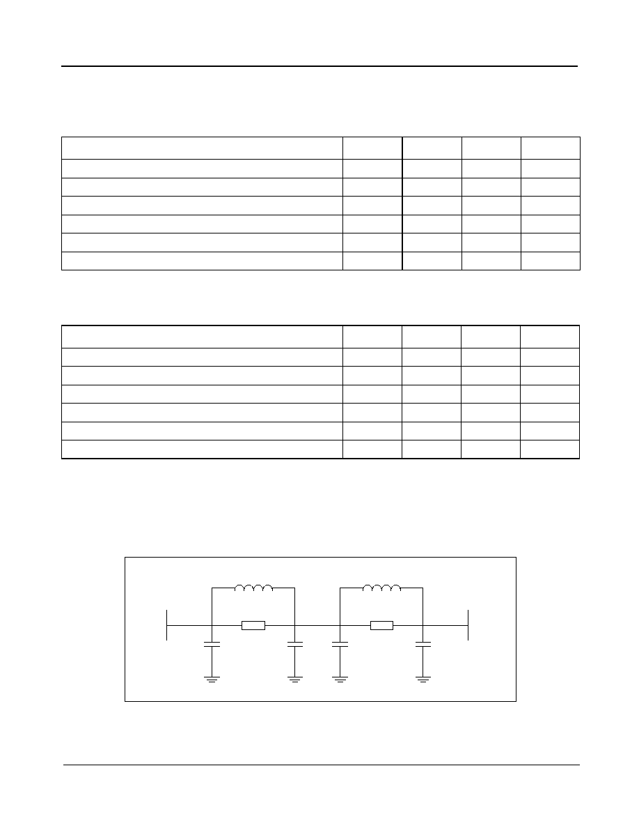
Figure 2 - Recommended Power Supply Filter
Parameter
Symbol
Min.
Max.
Unit
Supply voltage
V
CC
-0.3
4.0
V
Differential input voltage amplitude
1
1. Differential input voltage amplitude is defined as
V =
DIN+
-
DIN-
.
V
1.2
V
Voltage on any pin
V
PIN
-0.3
V
CC
+ 0.3
V
Relative humidity (non-condensing)
M
OS
5
95
%
Storage temperature
T
STG
-40
100
∞
C
ESD resistance
V
ESD
±1
kV
Parameter
Symbol
Min.
Max.
Unit
Power supply voltage
V
CC
3.135
3.465
V
Operating case temperature
T
CASE
0
80
∞
C
Signalling rate (per channel)
1
1. Data patterns are to have maximum run lengths and DC balance shifts no worse than that of a Pseudo Random Bit Sequence of
length 2
23
-1 (PRBS-23). Information on lower bit rates and longer run lengths are available on request.
f
D
1.0
2.7
Gbps
Link distance
2
2. For maximum distance, see Table 4.
LD
2
m
Data I/O DC blocking capacitors
3
3. For AC-coupling, DC blocking capacitors external to the module with a minimum value of 100 nF is recommended.
C
BLK
100
nF
Power supply noise
4
4. Power supply noise is defined at the supply side of the recommended filter for all V
CC
supplies over the frequency range of 500 Hz
to 2700 MHz with the recommended power supply filter in place.
V
NPS
200
mV
p-p
Host
Vcc
R1 100
C1
10
µ
F
C2
10
µ
F
L1 1
µ
H
R2 1.0 k
C3
0.1
µ
F
C4
0.1
µ
F
L2 6.8 nH
Module
Vcc

ZL60301
Data Sheet
5
Zarlink Semiconductor Inc.
Transmitter Specifications
All parameters below require operating conditions according to "Recommended Operating Conditions" on page 4.
Parameter
Symbol
Min.
Max.
Unit
Optical Parameters
Launch power (50/125
µ
m MMF)
1
1. The output optical power is compliant with IEC 60825-1 Amendment 2, Class 1M Accessible Emission Limits.
P
OUT
-8
-2
dBm
Extinguished output power
P
OFF
-30
dBm
Extinction ratio
2
2. The extinction ratio is measured at 622 Mbps.
ER
6
dB
Optical modulation amplitude
3
3. Informative. Corresponds to P
OUT
= -8 dBm and ER = 6 dBm.
OMA
0.30
mW
Center wavelength
C
830
860
nm
Spectral width
4
4. Spectral width is measured as defined in EIA/TIA-455-127 Spectral Characterization of Multimode Laser Diodes.
0.85
nm
rms
Relative intensity noise OMA
5
5. Corresponds to a Relative Intensity Noise (RIN) of -120 dB/Hz.
RIN
12
OMA
-116
dB/Hz
Optical output rise time (20 - 80%)
t
RO
150
ps
Optical output fall time (20 - 80%)
t
FO
150
ps
Total jitter contributed (peak to peak)
6
6. Total jitter equals TP1 to TP2 as defined in IEEE 802.3 clauses 38.2 and 38.6 (Gigabit Ethernet).
TJ
120
ps
Deterministic jitter contributed (peak to peak)
DJ
50
ps
Channel to channel skew
7
7. Channel skew is defined for the condition of equal amplitude, zero ps skew signals applied to the transmitter inputs.
t
SK
100
ps
Electrical Parameters
Power dissipation
P
D
500
mW
Supply current
I
CC
150
mA
Differential input voltage amplitude (peak to peak)
8
8. Differential input voltage is defined as the peak to peak value of the differential voltage between DIN+ and DIN-. Data inputs are CML
compatible.
V
IN
200
800
mV
p-p
Differential input impedance
9
9. Differential input impedance is measured between DIN+ and DIN-.
Z
IN
80
120
Electrical input rise time (20 - 80%)
t
RE
160
ps
Electrical input fall time (20 - 80%)
t
FE
160
ps

ZL60301
Data Sheet
6
Zarlink Semiconductor Inc.
Classified in accordance with IEC 60825-1/A2:2001, IEC 60825-2 : 2000
Class 1M Laser Product
Emited wavelength: 840 nm
Figure 3 - Differential CML Input Equivalent Circuit
50
50
13k
11k
V
EE
V
CC
DIN+
DIN-

ZL60301
Data Sheet
7
Zarlink Semiconductor Inc.
Transmitter Control and Status Signal Requirements
The following table shows the timing relationships of the status and control signals of the transmit section.
Parameter
Symbol
Min.
Typ.
Max.
Unit
Control input voltage high
1
1. Applies to control signals RESET, Tx_DIS and Tx_EN.
V
IH
2.1
V
Control input voltage low
V
IL
0.62
V
Control pull-up resistor
2
2. Applies to control signals RESET and Tx_EN. Internal pull-up resistor.
R
PU
10
k
Control pull-down resistor
3
3. Applies to control signal Tx_DIS. Internal pull-down resistor.
R
PD1
10
k
Status output voltage low
4, 5
4. Applies to status signal FAULT. Internal pull-down to V
EE
.
5. With status output sink current max. 2 mA.
V
OL
0.4
V
Status pull-down resistor
4
R
PD2
10
k
FAULT assert time
T
FA
100
µ
s
FAULT lasers off
T
FD
100
µ
s
RESET duration
T
TDD
10
µ
s
RESET assert time
T
OFF
5
10
µ
s
RESET de-assert time
T
ON
100
ms
Tx_EN assert time
T
TEN
1
ms
Tx_EN de-assert time
T
TD
5
10
µ
s
Tx_DIS assert time
T
TD
5
10
µ
s
Tx_DIS de-assert time
T
TEN
1
ms

ZL60301
Data Sheet
8
Zarlink Semiconductor Inc.
Transmitter Control and Status Timing Diagrams
The following figures show the timing relationships of the status and control signals of the transmit section.
Figure 4 - Transmitter Power-up Sequence
Figure 5 - Transmitter Fault Signal Timing Diagram
RESET: floating or high
Transmitter Not Ready
Normal operation
V
CC
T
TEN
Tx Output [0:3]
Data [0:3]
No Fault
Fault
FAULT
T
FA
T
FD
Tx Output [0:3]
Data [0:3]
ZL60301
Data Sheet
9
Zarlink Semiconductor Inc.
Figure 6 - Transmitter Reset Signal Timing Diagram
Figure 7 - Transmitter Enable and Disable Timing Diagram
Tx_DIS High
Tx_DIS Low
Tx_EN High
Transmitter disabled
Normal operation
Tx_EN Low
Transmitter disabled
Transmitter disabled
Table 1 - TruthTable for Transmitter Operation (Pre-condition: RESET floating or HIGH)
Transmitter Not Ready
Normal operation
FAULT
T
ON
Tx Output [0:3]
Data [0:3]
RESET
T
TDD
Tx_EN
Data [0:3]
Lasers
off
T
TD
Normal operation
Tx Off
Tx_DIS
Lasers
off
Data [0:3]
T
TD
Normal operation
Tx Off
Data [0:3]
Tx_EN
T
TEN
Normal operation
Transmitter Not Ready

ZL60301
Data Sheet
10
Zarlink Semiconductor Inc.
Receiver Specifications
All parameters below require operating conditions according to "Recommended Operating Conditions" on page 4
and a termination load of 100
differential at the electrical output.
Parameter
Symbol
Min.
Max.
Unit
Optical Parameters
Input optical power
1
1. Receive power for a channel is measured for a BER of 10
-12
and worst case extinction ratio. P
IN
(Min) is measured using a fast
rise/fall time source with low RIN and adjacent channel(s) operating with incident power of 6 dB above P
IN
(Min).
P
IN
-16
-2
dBm
Center wavelength
C
830
860
nm
Return loss
2
2. Return loss is measured as defined in TIA/EIA-455-107A Determination of Component Reflectance or Link/System Return Loss Us-
ing a Loss Test Set.
RL
12
dB
Stressed receiver sensitivity
3
3. The stressed receiver sensitivity is measured using PRBS 2
23
-1 pattern, 2.6 dB inter-symbol interference, ISI (Min), 30 ps duty cycle
dependent deterministic jitter, DCD DJ (Min), and 6 dB extinction ratio, ER (Min) (ER penalty = 2.2 dB). All channels not under test
are receiving signals with an average input power of 6 dB above P
IN
(Min).
P
SS
-11.7
dBm
Channel to channel skew
4
4. Channel skew is defined for the condition of equal amplitude, zero ps skew signals applied to the receiver inputs.
t
SK
100
ps
Signal detect assert
P
SA
-17
dBm
Signal detect de-assert
P
SD
-31
dBm
Electrical Parameters
Power dissipation
P
D
500
mW
Supply current
I
CC
150
mA
Differential output voltage amplitude (peak to peak)
5
5. Differential output voltage is defined as the peak to peak value of the differential voltage between DOUT+ and DOUT- and measured
with a 100
differential load connected between DOUT+ and DOUT-. Data outputs are CML compatible.
V
OUT
500
800
mV
p-p
Output differential load impedance
6
6. See Figure 13.
Z
L
80
120
Stressed receiver eye opening
7
7. The stressed receiver eye opening represents the eye at TP4 as defined in IEEE 802.3 clauses 38.2 and 38.6 (Gigabit Ethernet).
The stressed receiver eye opening is measured using PRBS 2
23
-1 pattern, 2.6 dB ISI min, 30 ps DCD DJ min, 6 dB ER min and an
average input power of -11.2 dBm (0.5 dB above minimum stressed receiver sensitivity as defined in IEEE 802.3 clause 38.6). All
channels not under test are receiving signals with an average input power of 6 dB above P
IN
(Min).
P
SE
0.3
UI
Electrical output rise time (20 - 80%)
t
RE
160
ps
Electrical output fall time (20 - 80%)
t
FE
160
ps

ZL60301
Data Sheet
11
Zarlink Semiconductor Inc.
Receiver Control and Status Signal Requirements
The following table shows the timing relationships of the status and control signals of the receive section.
Receiver Control and Status Timing Diagrams
The following figures show the timing relationships of the status and control signals of the receive section.
Figure 8 - Receiver Enable Signal Timing Diagram
Parameter
Symbol
Min.
Typ.
Max.
Unit
Control input voltage high
1
1. Applies to control signals Rx_EN, SQ_EN.
V
IH
2.0
V
Control input voltage low
1
V
IL
0.9
V
Control input pull-up current
1
I
IN
10
100
µ
A
Status output voltage low
2, 3
2. Applies to status signal Rx_SD. Internal pull-up to V
CC
.
3. With status output sink current max 2 mA.
V
OL
0.4
V
Status output pull-up resistor
2
R
PU
3.25
k
Receiver signal detect assert time
T
SD
50
200
µ
s
Receiver signal detect de-assert time
T
LOS
50
200
µ
s
Receiver enable assert time
T
RXEN
33
ms
Receiver enable de-assert time
T
RXD
5
µ
s
Normal Operation
Rx Off
Rx_EN
T
RXD
I
CC

ZL60301
Data Sheet
12
Zarlink Semiconductor Inc.
Figure 9 - Receiver Signal Detect Timing Diagram
Transceiver Module Signals
The pluggable parallel optical transceiver uses a 100 position FCI MegArray electrical connector
(FCI PN: 84513-101), and an industry standard MTP
(
MPO) optical receptacle compliant with
IEC 61754-7.
K
J
H
G
F
E
D
C
B
A
1
DOUT00-
V
EE
Rx
DOUT03+
V
EE
Rx
V
EE
Rx
V
EE
Tx
V
EE
Tx
DIN03-
V
EE
Tx
DIN00+
2
DOUT00+
V
EE
Rx
DOUT03-
V
EE
Rx
V
EE
Rx
V
EE
Tx
V
EE
Tx
DIN03+
V
EE
Tx
DIN00-
3
V
EE
Rx
V
EE
Rx
V
EE
Rx
V
EE
Rx
V
EE
Rx
V
EE
Tx
V
EE
Tx
V
EE
Tx
V
EE
Tx
V
EE
Tx
4
DOUT01+
V
EE
Rx
DOUT02-
NIC
NIC
NIC
NIC
DIN02+
V
EE
Tx
DIN01-
5
DOUT01-
V
EE
Rx
DOUT02+
NIC
NIC
NIC
NIC
DIN02-
V
EE
Tx
DIN01+
6
V
EE
Rx
V
EE
Rx
V
EE
Rx
NIC
NIC
NIC
NIC
V
EE
Tx
V
EE
Tx
V
EE
Tx
7
V
CCB
Rx
V
CCB
Rx
V
CCB
Rx
NIC
NIC
NIC
NIC
V
CC
Tx
V
CC
Tx
V
CC
Tx
8
NIC
DNC
DNC
DNC
RX_EN
TX_DIS
TX_EN
DNC
DNC
DNC
9
NIC
DNC
DNC
SD
SQ_EN
RESET
FAULT
DNC
DNC
DNC
10
V
CCA
Rx
V
CCA
Rx
V
EE
Rx
NIC
NIC
NIC
NIC
V
EE
Tx
V
CC
Tx
V
CC
Tx
Table 2 - Transceiver Pinout Assignments (Top view, toward MPO/MTP
connector end)
(10x10 array, 1.27 mm pitch)
Module front view - MTP key up
Tx0
Tx1
Tx2
Tx3
-
-
-
-
Rx3
Rx2
Rx1
Rx0
Host printed circuit board
Table 3 - Transceiver Optical Channel Assignment
Signal
No Signal
Rx_SD
T
LOS

ZL60301
Data Sheet
13
Zarlink Semiconductor Inc.
Transceiver Pin Description
The transceiver module case is electrically isolated from Transmitter signal common and Receiver signal common.
Connection through mounting screw holes or frontplate whichever is applicable. Make the appropriate electrical
connection for EMI shield integrity.
Signal Name
Type
Description
Comments
DIN[0:3] +/-
Data input
Transmitter data in, channel 0 to 3
Internal differential
termination at 100
.
V
CC
Tx
Transmitter power supply rail
V
EE
Tx
Transmitter signal common. All transmitter
voltages are referenced to this potential unless
otherwise stated.
Directly connect these pads
to the PC board transmitter
signal ground plane.
TX_EN
Control
input
Transmitter enable.
HIGH: normal operation
LOW: disable transmitter
Active high, internal pull-up.
See Table 1.
TX_DIS
Control
input
Transmitter disable.
HIGH: disable transmitter
LOW: normal operation
Active high, internal pull-
down. See Table 1.
FAULT
Status
output
Transmitter fault.
HIGH: normal operation
LOW: laser fault detected on at least one channel
When active, all channels
are disabled. Clear by reset
signal. Internal pull-up.
RESET
Control
input
Transmitter reset.
HIGH: normal operation
LOW:reset to clear fault signal
Internal pull-up.
DOUT[0:3] +/-
Data
output
Receiver data out, channel 0 to 3.
V
CCA
Rx
PIN preamplifier power supply rail.
V
CCB
Rx
Receiver quantizer power supply rail.
V
EE
Rx
Receiver signal common. All receiver voltages
are referenced to this potential unless otherwise
stated.
Directly connect these pads
to the PC board receiver
signal ground plane.
RX_EN
Control
input
Receiver enable.
HIGH: normal operation
LOW: disable receiver
Internal pull-up.
RX_SD
Status
output
Receiver signal detect.
HIGH: valid optical input on all channels
LOW: loss of signal on at least one channel
Internal pull-up.
SQ_EN
Control
input
Squelch enable.
HIGH: squelch function enabled. Data OUT is
squelched on any channels that have loss of
signal
LOW: squelch function disabled
Internal pull-up.
DNC
Do not connect to any potential, including ground.
NIC
No internal connection.
ZL60301
Data Sheet
14
Zarlink Semiconductor Inc.
V
CCA
and V
CCB
Rx can be connected to the same power supply. However, to insure maximum receiver sensitivity
and minimize the impact of noise from the power supply, it is recommended to keep the power supplies separate
and to use the recommended power supply filtering network on V
CCA
Rx, see Figure 2.
Thermal Characteristics
There are three options for heat sinks depending on the cooling needs. They are:
1. Direct application without any attached external heat sink
2. Use a generic external heat sink specified by Zarlink
3. Use a customer designed external heat sink
In Figure 10 and Figure 11, the temperature rise and thermal resistance as a function of air velocity (free air velocity
at the top of the module) is shown for option 1 and 2. The thermal resistance is defined as the temperature
difference between the case temperature and ambient flowing air divided by the total heat dissipation of the
module.
Improved thermal properties can be achieved by using a larger heat sink especially if more height is available
(option 3). For this option, a more detailed discussion with Zarlink is recommended regarding heat sink design
attachment materials.
Figure 10 - Temperature Difference Between Ambient Flowing Air and Case at a Heat Dissipation
of 1.0 W
Tem perature rise at 1.0W
(Free stream air velocity)
0
4
8
12
16
0
1
2
3
4
5
Air velocity (m /s)
Temperature rise (K)
Option ZL60301/MLD
Option ZL60301/MJD

ZL60301
Data Sheet
15
Zarlink Semiconductor Inc.
Figure 11 - Thermal Resistance, as a Function of Air Velocity (the airflow is along the shortest
side of the module)
For any other orientation, the thermal resistance is 75-100% of the values shown above.
Therm al resistance to air
(Free stream air velocity)
0
5
10
15
0
1
2
3
4
5
Air velocity (m /s)
Thermal resistance (K/W)
Option ZL60301/MLD
Option ZL60301/MJD

ZL60301
Data Sheet
16
Zarlink Semiconductor Inc.
Regulatory Compliance
Eye safety
The maximum optical output power is specified to comply with Class 1M in accordance with IEC 60825
-
1:2001. In
addition the transmitter complies with FDA performance standards for laser products except for deviations pursuant
to Laser Notice No.50, dated July 26, 2001. No maintenance or service of the product may be performed.
Electrostatic discharge
The module is classified as Class 1 (> 1000 Volts) according to MIL
-
STD
-
883, test method 3015.7, with regards to
the electrical pads.
Electrostatic discharge immunity
The part withstand a 15 kV (air discharge) and 8 kV (contact discharge) either indirect or directly to receptacle;
tested according to IEC 61000
-
4
-
2, while in operation without addition of bit errors.
Electromagnetic Interference
Emission
The electromagnetic emission is tested in front of the module (module fitted with EMI shield), with the module
mounted in a frontplate cutout. The part is tested with FCC Part 15, 30
-
1000 MHz and 1 GHz to 5
th
harmonic of
the highest fundamental frequency (6.75 GHz), and is specified to be Class B with > 6 dB margin.
Immunity
The electromagnetic immunity is tested without a front panel or enclosure. The module specification is maintained
with an applied field of 10 V/m for frequencies between 10 kHz and 10 GHz, according to IEC 61000
-
4
-
3 and GR
-
1089
-
CORE.
Handling instructions
Cleaning the Optical Interface
A protective connector plug is supplied with each module. This plug should remain in place whenever a fiber cable
is not inserted. This will keep the optical port free from dust or other contaminants, which may potentially degrade
the optical signal. Before reattaching the connector plug to the module, visually inspect the plug and remove any
contamination. If the module's optical port becomes contaminated, it can be cleaned with high-pressure nitrogen
(the use of fluids, or physical contact, is not advised due to potential for damage).
Before a fiber cable connector is attached to the module, it is recommended to clean the fiber cable connector
using an optical connector cleaner, or according to the cable manufacturer's instructions. It is also recommended to
clean the optical port of the module with high-pressure nitrogen.
Connectors
For optimum performance, it is recommended that the number of insertions is limited to 50 for the electrical
MegArray connector and 200 for the optical MPO/MTP connector.
ESD handling
When handling the modules, precautions for ESD sensitive devices should be taken. These include use of ESD
protected work areas with wrist straps, controlled work-benches, floors etc.

ZL60301
Data Sheet
17
Zarlink Semiconductor Inc.
Link Reach
The following table lists the minimum reach distance of the pluggable parallel fiber optic transceiver for different
multi-mode fiber (MMF) types and bandwidths assuming worst case parameters. Each case allows for a maximum
of 2 dB per channel connection loss for patch cables and other connectors.
Link Model Parameters
The link reaches above have been calculated using the following link model parameters and Gigabit Ethernet link
model version 2.3.5 (filename: 5pmd047.xls).
Fiber Type
[core / cladding
µ
m]
Modal Bandwidth
@ 850 nm
[MHz*km]
Reach Distance
@ 1 Gbps
[m]
Reach Distance
@ 2.5 Gbps
[m]
Reach Distance
@ 2.7 Gbps
[m]
62.5/125 MMF
200
350
135
115
62.5/125 or 50/125 MMF
400
650
260
220
50/125 MMF
500
750
300
270
Table 4 - Link Reach for Different Fiber Types and Data Rates
Parameter
Symbol
Value
Unit
Mode partition noise k-factor
k
0.3
Modal noise
MN
0.3
dB
Dispersion slope parameter
S
O
0.11
ps/nm
2
*km
Wavelength of zero dispersion
U
O
1320
nm
Attenuation coefficient at 850 nm
dB
3.5
dB/km
Conversion factor
C1
480
ns.MHz
Q-factor [BER 10
-12
]
Q
7.04
TP4 eye opening
0.3
UI
DCD allocation at TP3
DCD DJ
0.08
UI
RMS baseline wander S.D.
BLW
0.025
RIN coefficient
k
RIN
0.70
Conversion factor
c_rx
329
ns.MHz

ZL60301
Data Sheet
18
Zarlink Semiconductor Inc.
Electrical Interface - Application Examples
Figure 12 - Recommended Differential CML Input Interface
Figure 13 - Recommended Differential CML Output Interface
Z
OUT
=100
Differential
Recommended CML output
Z
0
=100
Differential
Z
IN
=100
Differential
Transmitter CML input
100nF
100nF
Host PCB
Receiver CML output
Z
0
=100
Differential
Z
TERM
=100
Differential
Recommended CML input
100nF
100nF
Host PCB
Z
L

FRONT VIEW ( 2 : 1 )
© Zarlink Semiconductor 2002. All rights reserved.
ISSUE
ACN
DATE
APPRD.
Previous package codes
Title
Drawing type
Package code
* For details of the module, see separate data sheet and/or package drawing.
Projection Method
2
104518 rev2
11-AUG-04
MD/MA
104518
ML
External Heatink
Module *
Washplug Assembly
27
7
,
6
1
5
,
5
M
A
X
8,5
1,5 (5x)
17
0
,
9
NOTES:-
1, All dimensions in mm.
2, Tolerancing per ASME Y14.5M-1994
5
,
8
12,6
Package Drawing,
Module Layout External Heatsink

© Zarlink Semiconductor 2002. All rights reserved.
ISSUE
ACN
DATE
APPRD.
Previous package codes
Title
Drawing type
Package code
1
JS004296R1A
12-JUN-03
TD/BE
JS004296
Package drawing - module layout
MJ
NOTES:-
1. All dimensions in mm.
2. Tolerancing per ASME Y14.5M-1994.
© Zarlink Semiconductor 2002. All rights reserved.
ISSUE
ACN
DATE
APPRD.
Previous package codes
Title
Drawing type
Package code
1
JS004296R1A
12-JUN-03
TD/BE
JS004296
Package Drawing,
MJ
Host circuit board footprint layout
NOTES:-
1. All dimensions in mm.
2. Tolerancing per ASME Y14.5M-1994.

www.zarlink.com
Information relating to products and services furnished herein by Zarlink Semiconductor Inc. or its subsidiaries (collectively "Zarlink") is believed to be reliable.
However, Zarlink assumes no liability for errors that may appear in this publication, or for liability otherwise arising from the application or use of any such
information, product or service or for any infringement of patents or other intellectual property rights owned by third parties which may result from such application or
use. Neither the supply of such information or purchase of product or service conveys any license, either express or implied, under patents or other intellectual
property rights owned by Zarlink or licensed from third parties by Zarlink, whatsoever. Purchasers of products are also hereby notified that the use of product in
certain ways or in combination with Zarlink, or non-Zarlink furnished goods or services may infringe patents or other intellectual property rights owned by Zarlink.
This publication is issued to provide information only and (unless agreed by Zarlink in writing) may not be used, applied or reproduced for any purpose nor form part
of any order or contract nor to be regarded as a representation relating to the products or services concerned. The products, their specifications, services and other
information appearing in this publication are subject to change by Zarlink without notice. No warranty or guarantee express or implied is made regarding the
capability, performance or suitability of any product or service. Information concerning possible methods of use is provided as a guide only and does not constitute
any guarantee that such methods of use will be satisfactory in a specific piece of equipment. It is the user's responsibility to fully determine the performance and
suitability of any equipment using such information and to ensure that any publication or data used is up to date and has not been superseded. Manufacturing does
not necessarily include testing of all functions or parameters. These products are not suitable for use in any medical products whose failure to perform may result in
significant injury or death to the user. All products and materials are sold and services provided subject to Zarlink's conditions of sale which are available on request.
Purchase of Zarlink's I
2
C components conveys a licence under the Philips I
2
C Patent rights to use these components in and I
2
C System, provided that the system
conforms to the I
2
C Standard Specification as defined by Philips.
Zarlink, ZL and the Zarlink Semiconductor logo are trademarks of Zarlink Semiconductor Inc.
Copyright Zarlink Semiconductor Inc. All Rights Reserved.
TECHNICAL DOCUMENTATION - NOT FOR RESALE
For more information about all Zarlink products
visit our Web Site at