
- 1 -
ZEN2002AP
P ROGRAMMABLE
U N IVE RSAL
COU N TE R
Description
is a 24 bit pr ogr a m m a ble u n iver sa l cou n t er LSI .
ZENIC INC. ZEN2002AP
TH E
cou n t s ph a se-sh ift ed sign a ls a n d u p/down pu lse sign a ls, gen er a t ed fr om r ot a r y en coder s or
ZEN2002AP
lin ea r sca les.
Sin ce t h e cou n t er r espon se speed is a s h igh a s 20MH z(MAX),t h e
is u sed in a va r iet y of h igh speed
ZEN2002AP
ser vices in clu din g digit a l ser vo con t r ol a n d pr ecision m ea su r em en t .
TH E
is pr ovided wit h a fu n ct ion wh ich m on it or s t h e in pu t sign a ls a n d det ect s a n y a bn or m a l in pu t
ZEN2002AP
a ccom pa n ied wit h n oise or ot h er dist u r ba n ces, so t h a t t h e r elia bilit y of cou n t ed va lu es a r e secu r ed.
1, Features
24 bit bin a r y u p/down cou n t er .
Cou n t er r espon se speed:
20MH z.(MAX.) ( CLK f = 20MH z a t 50% du t y)
0
In pu t fr equ en cy of cou n t pu lse.
P h a se-sh ift ed sign a l in pu t :
A/B ph a se in pu t DC ~ 5MH z.
(less t h a n f
1/4)
0
~
U p/down pu lse sign a l in pu t :
U p/down in pu t DC ~ 10MH z
(less t h a n f
1/2)
0
~
CLK fr equ en cy DC ~ 20MH z.
(MAX.: du t y r a t io 50%)
Dir ect ion r ecogn it ion for u p/down cou n t in g.
Abn or m a l in pu t det ect ion cir cu it .
P r eloa d r egist er for t h e u p/down cou n t er .
La t ch r egist er for t h e u p/down cou n t er .
Refer en ce va lu e - cou n t va lu e coin ciden ce
det ect ion fu n ct ion .
Mom en t a r y ou t pu t : TTL
In t er r u pt ou t pu t (la t ch ed) : open collect or
On -ch ip st a t u s r egist er .
Cou n t er oper a t ion m ode.
E dge eva lu a t ion select ion : sin gle/dou ble/qu a d
(on ly for ph a se-sh ift ed sign a l in pu t )
Cou n t dir ect ion select ion .
Cou n t er clea r con t r ol:syn ch r on ou s/
a syn ch r on ou s clea r .
F ixed/va r ia ble edge clea r .
8 bit da t a bu s.
Low power CMOS t ech n ology.
TTL com pa t ible.
Sin gle 5V power su pply.
28 pin DIP .
2, Typical Applications
N C m a ch in e t ools
P r ecision posit ion er s
Robot a r m con t r oller s
Speed con t r oller s for r ot a t in g m a ch in es
E lect r on ic ga u ges
F r equ en cy cou n t er s
Pin configuration
(Top view)
VSS
1
28
VDD
CLK
2
27
INT
RESET
3
26
EQ
CE
4
25
UD/AB
Z
C/D
5
24
DIR
E
RD
6
23
VSS
N
WR
7
22
A/UP
2
LD
8
21
B/DN
0
LT
9
20
Z/CLR
0
D0
10
19
D7
2
D1
11
18
D6
A
D2
12
17
D5
P
D3
13
16
D4
VSS
14
15
VDD
ZENIC Inc.

- 2 -
ZEN2002AP
3, Block Diagram
CE
Command
C/D
register
RD
Control
(8bit)
WR
logic
LT
LD
Status
register
(8bit)
Reference
register
(24bit)
Interrupt
control logic
INT
Comparator
(24bit)
EQ
Latch register
(24bit)
UD/AB
Up/down counter
DIR
(24bit)
UP PULSE
A/UP
Phase
DOWN PULSE
B/DN
discrimi-
COUNTER CLEAR
Z/CLR
nation
RESET
Preload register
CLK
(24bit)
VDD
VSS
D7 D0
~
ZENIC Inc.

- 3 -
ZEN2002AP
4, Block function
1) Up/down counter
It is presettable up/down binary counter of 24 bit length.
The count value can be read out from the latch register via the data bus without influencing to the count operation.
The counter value is initialized by loading the preload register(24bits) or via the data bus every 8 bits.
2) Reference register
It is a writing register of 24 bit length.
The written data is compared by the comparator with the count value of the up/down counter.
3) Comparator
It is a digital comparator of 24 bit length.
The data of the reference register is always compared with the counter value of the up/down counter and the result is
output to EQ(26Pin), the status register, and the interruption control logic.
4) Preload register
It is a data register of 24 bit length.
Its data is loaded into the up/down counter by the external signal LD(8Pin) or the command(load instruction).
5) Latch register
It is a data register only for reading 24 bit length.
It latch the count value of the up/down counter by the external signal LT(9Pin) or the command(latch instruction).
6) Command register
It is a register for the command writing. ( 8 bits )
The controls of loading instruction, latch instruction, count clear control, and register (byte) selection and count mode
changes, etc. are done by using this register.
7) Status register
It is a register for the status reading. ( 8 bits )
It monitors the state of abnormal input detection, the state of input signal(A,B,Z), the state of the latch register,
count direction, the state of coincidence detection(count value = preset value), and the state of interruption output
(INT).
8) Phase distcrimination logic
The count pulse for the up/down counter is generated from the input signal of A/UP(22Pin) and B/DN(21Pin).
9) Control logic
The read/write timing control, the decoding about the command data, and the status flag control.
ZENIC Inc.
- 4 -
ZEN2002AP
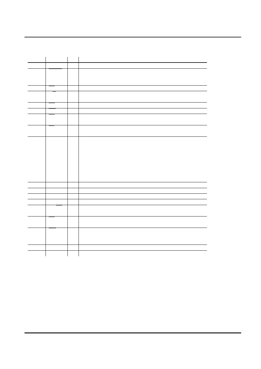
5, Pin Description
Pin No.
Signal
I/O
Function
2
CLK
I
System clock
3
RESET
I
System reset
Up/down counter, phase discrimination logic, command register
and the status register are initialized.
4
CE
I
Chip enable
5
C/D
I
Command/data select
"High":command/status
"Low":data
6
RD
I
Read strobing
7
WR
I
Write strobing
8
LD
I
Data loading
The data of the preload register is loaded to the up/down counter
9
LT
I
Count data latch
The count value of the up/down counter is latched to the latch register.
10
D0
I/O
Data bus
11
D1
Bidirectional data bus ( 8 bits ).
12
D2
It is used to transmit and receive the command, status and data.
13
D3
16
D4
17
D5
18
D6
19
D7
20
Z/CLR
I
Counter clear
21
B/DN
I
Count pulse input B
22
A/UP
I
Count pulse input A
24
DIR
I
Count direction selection
25
UD/AB
I
Input signal selection
Selection up/down or phase-shifted pulse
26
EQ
O
Coincidence detection output
Coincidence detection output of count value and preset value of reference register.
27
INT
O
Interruption output
When the coincidence of the count value and the preset value is detected, it outputs.
It maintains to reset or the reset command execution.
1
VSS
Power supply ( 5v )
15
VDD
Ground ( 0v )
ZENIC Inc.

- 5 -
ZEN2002AP
6, Basic operation
The read/write operation is selected according to CE, C/D, RD, and WR.
CE
C/D
RD
WR
Operation
H
-
-
-
Disable
L
L
L
H
The data reading
L
L
H
L
The data writing
L
H
L
H
Status reading
L
H
H
L
Command writing
1) Selection of count pulse input
UD/AB
Input pulse signal
A/UP
B/DN
H
Up/down pulse
Up pulse
Down pulse
L
Phase-shifted pulse
Phase-A pulse
Phase-B pulse
2) Access pointer
The internal register is selected by setting the access pointer of the command register. Once setting the pointer,
it is incremented automatically after reading or writing 1 byte data. ( automatical increment function )
3) Abnormal input detection
The function is to check whether it is normal state transition () when the phase-shifted pulse is input.
When the abnormal state transition happens , D7 of the status register becomes "H".
AB
AB
: noamal transition
01
11
: abnormal transition
00
10
Example of causing abnormal
When it is not possible to sample signal accurately
a.
because the pulse input frequency exceeded 1/4 of the system clock frequency.
b. When you pick up noise.
4) Selection of count edge ( C = count , nc = no count )
Up/down pulse input
UP
DN
Single
C
C
C
C
nc
Phase-shifted pulse input
( CW (phase-A preceding))
( CCW (phase-B preceding))
A
A
B
B
Single
C
nc nc nc
Single
nc nc
nc
C
Double
C
nc
C nc
Double
nc C
nc
C
Quad
C
C
C
C
Quad
C
C
C
C
ZENIC Inc.