SUMMARY
V
R
= 40V; I
FAV
= 510mA;
V
F
= 405mV typ @ 100mA; I
R
= 7µA typ @ 30V
DESCRIPTION
Packaged in the SOD523 package this addition to the
Zetex Schottky diode range offers an ideal low VF/IR
performance combined with a low package height of
0.9mm making the device suitable for various
converter, charger, and LED driver circuits.
FEATURES
∑
Vr = 40V
∑
Low V
F
∑
350mA continuous current rating
∑
Low profile SOD523 package (0.9mm)
∑
100% matte tin plated external leads
APPLICATIONS
∑
DC - DC converters
∑
Mobile telecomms
∑
Charger circuits
∑
LED driver circuits
∑
MOSFET voltage protection circuits
∑
High frequency rectification
Prior to May 2005 (Pb free conversion date) a prefix `u'
will be applied to the part numberto denote Pb free for
ordering purposes only.
DEVICE MARKING
∑
35
ZHCS350
ISSUE 1 - AUGUST 2004
SOD523 40V LOW V
F
SCHOTTKY BARRIER DIODE
1
SOD523
PINOUT
TOP VIEW
DEVICE
REEL
SIZE
TAPE WIDTH
QUANTITY PER
REEL
ZHCS350TA
7"
8mm embossed
3,000 units
ZHCS350TC
13"
8mm embossed
10,000 units
ORDERING INFORMATION
ZHCS350
ISSUE 1 - AUGUST 2004
2
PARAMETER
SYMBOL
LIMIT
UNIT
Continuous Reverse Voltage
V
R
40
V
Continuous Forward Current
I
F
350
mA
Average Peak Forward Current; D.C. = 50%
I
FAV
510
mA
Non Repetitve Forward Current t < 100µS
< 10mS
I
FSM
4.2
910
A
mA
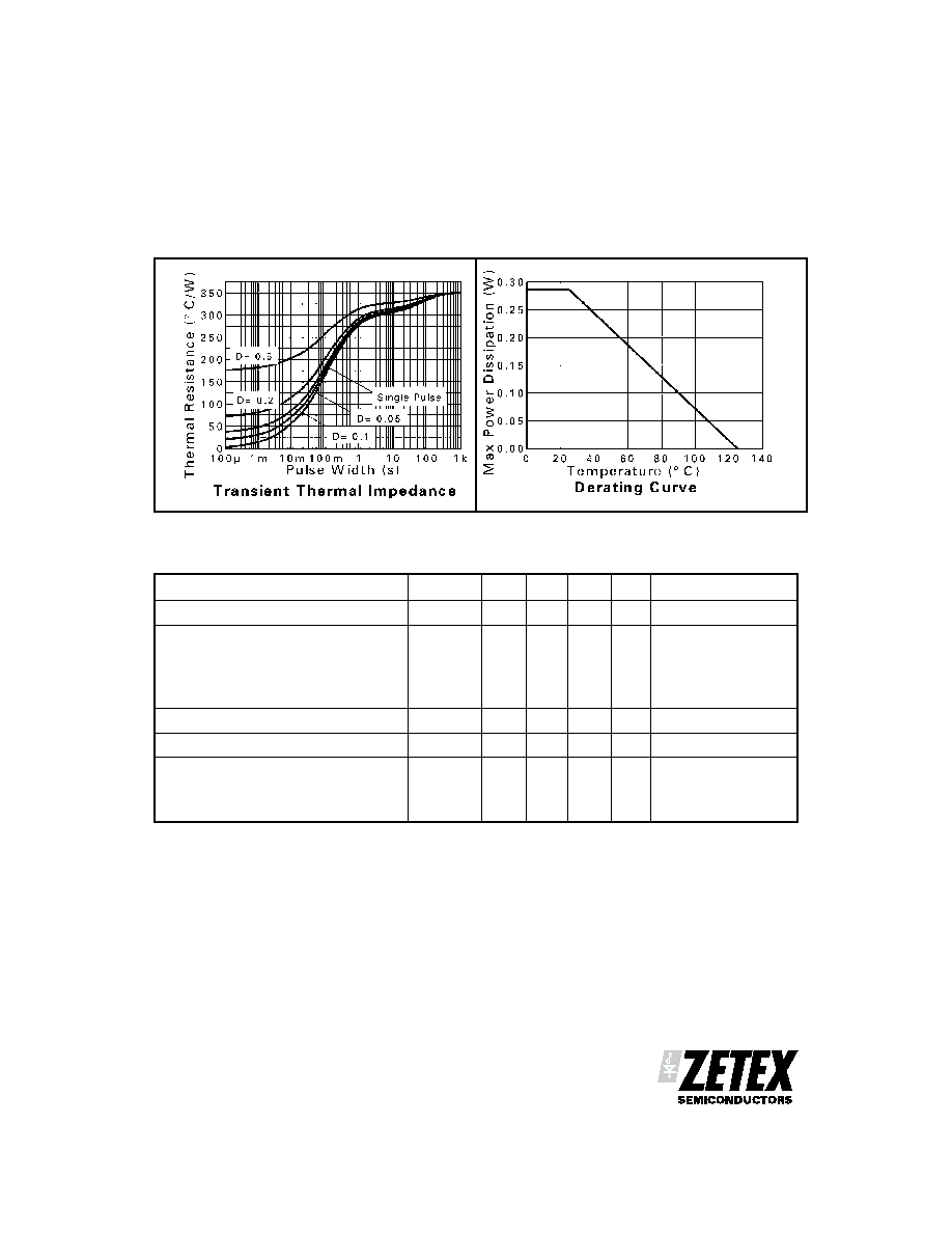
Power Dissipation at TA=25∞C
(a)
P
D
285
mW
Power Dissipation at TA=25∞C
(b)
P
D
330
mW
Storage Temperature Range
Tstg
-55 to +150
∞C
Junction Temperature
Tj
125
∞C
ABSOLUTE MAXIMUM RATINGS
PARAMETER
SYMBOL
VALUE
UNIT
Junction to Ambient
(a)
R
JA
350
∞C/W
Junction to Ambient
(b)
R
JA
303
∞C/W
NOTES
(a) For a single device surface mounted on 25mm x 25mm x 1.6mm FR4 PCB with high coverage of 1oz copper in still air conditions.
(b) As (a) above measured at t<5 secs.
THERMAL RESISTANCE
ZHCS350
ISSUE 1 - AUGUST 2004
3
PARAMETER
SYMBOL
MIN.
TYP.
MAX.
UNIT CONDITIONS
Reverse Breakdown Voltage
V
(BR)R
40
60
V
I
R
=100 A
Forward Voltage
V
F
300
335
405
730
325
370
460
810
mV
mV
mV
mV
I
F
=30mA*
I
F
=50mA*
I
F
=100mA*
I
F
= 350mA*
Reverse Current
I
R
7
12
A
V
R
=30V
Diode Capacitance
C
D
3.3
6
pF
f=1MHz; V
R
=25V
Reverse Recovery Time
t
rr
1.6
nS
Switched from
I
F
=100mA to I
R
=100mA
Measured at I
R
=10mA
ELECTRICAL CHARACTERISTICS (at T
amb
= 25∞C unless otherwise stated)
NOTES
* Measured under pulsed conditions. Pulse width=300 S. Duty cycle
%
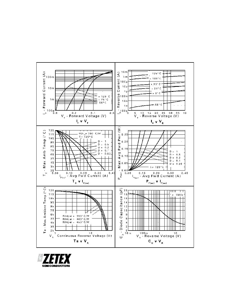
CHARACTERISTICS
ZHCS350
ISSUE 1 - AUGUST 2004
5
Europe
Zetex GmbH
Streitfeldstraþe 19
D-81673 M¸nchen
Germany
Telefon: (49) 89 45 49 49 0
Fax: (49) 89 45 49 49 49
europe.sales@zetex.com
Americas
Zetex Inc
700 Veterans Memorial Hwy
Hauppauge, NY 11788
USA
Telephone: (1) 631 360 2222
Fax: (1) 631 360 8222
usa.sales@zetex.com
Asia Pacific
Zetex (Asia) Ltd
3701-04 Metroplaza Tower 1
Hing Fong Road, Kwai Fong
Hong Kong
Telephone: (852) 26100 611
Fax: (852) 24250 494
asia.sales@zetex.com
Corporate Headquarters
Zetex Semiconductors plc
Lansdowne Road, Chadderton
Oldham, OL9 9TY
United Kingdom
Telephone (44) 161 622 4444
Fax: (44) 161 622 4446
hq@zetex.com
These offices are supported by agents and distributors in major countries world-wide.
This publication is issued to provide outline information only which (unless agreed by the Company in writing) may not be used, applied or reproduced
for any purpose or form part of any order or contract or be regarded as a representation relating to the products or services concerned. The Company
reserves the right to alter without notice the specification, design, price or conditions of supply of any product or service.
For the latest product information, log on to www.zetex.com
© Zetex Semiconductors plc 2004
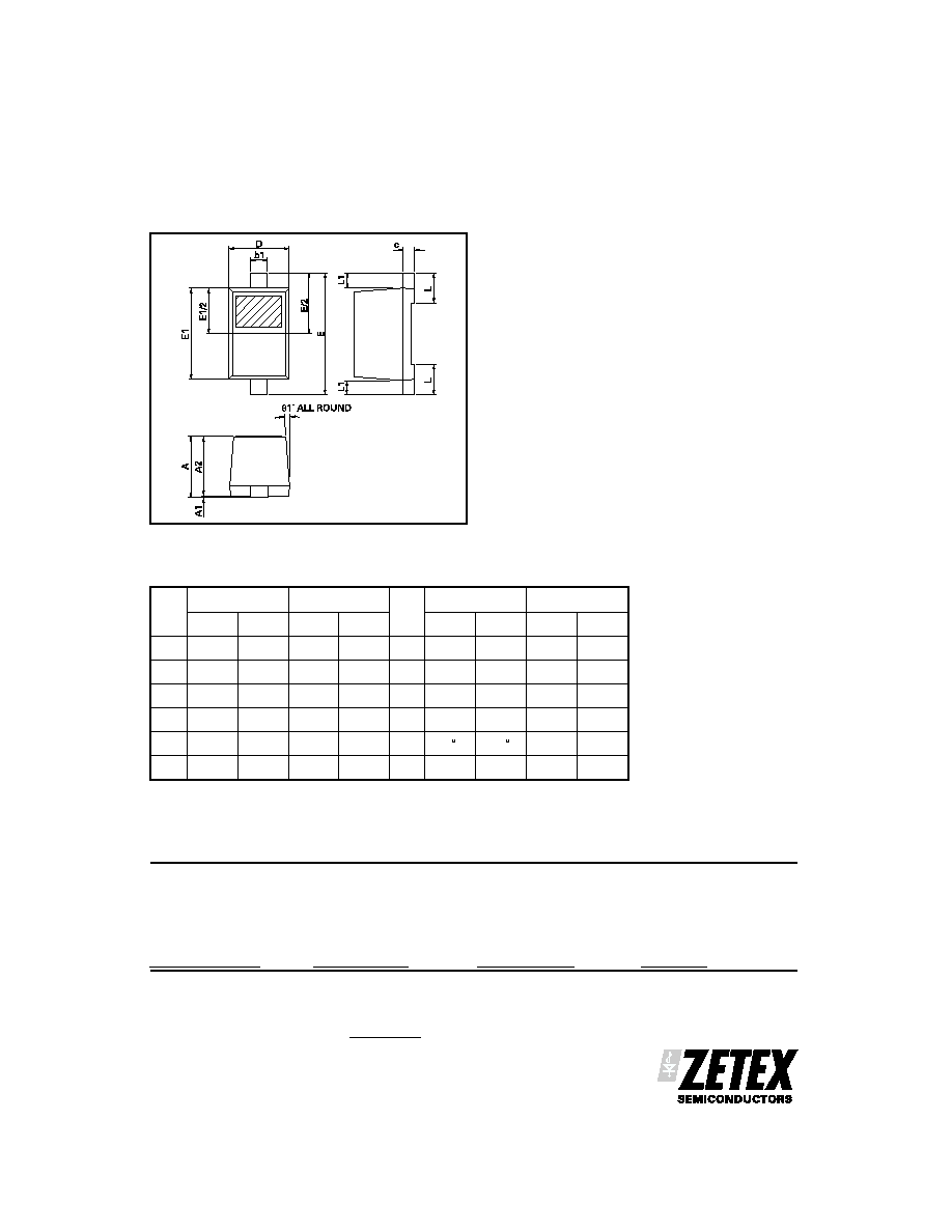
Controlling dimensions are in millimeters. Approximate conversions are given in inches
PACKAGE OUTLINE
DIM
Millimeters
Inches
DIM
Millimeters
Inches
Min
Max
Min
Max
Min
Max
Min
Max
A
≠
0.800
≠
0.0314
E
1.500
1.700
0.0590
0.0669
A1
0.000
0.100
0.000
0.0039
E1
1.100
1.300
0.0433
0.0511
A2
0.600
0.800
0.0236
0.0314
L
0.200
0.400
0.0078
0.0157
b1
0.160
0.300
0.0062
0.0118
L1
0.170
0.230
0.0066
0.0090
c
0.080
0.220
0.0031
0.0086
1
4
10
4
10
D
0.700
0.900
0.0275
0.0354
PACKAGE DIMENSIONS