 | –≠–ª–µ–∫—Ç—Ä–æ–Ω–Ω—ã–π –∫–æ–º–ø–æ–Ω–µ–Ω—Ç: ZHX2010 | –°–∫–∞—á–∞—Ç—å:  PDF PDF  ZIP ZIP |

ZiLOG Worldwide Headquarters ∑ 532 Race Street ∑ San Jose, CA 95126-3432
Telephone: 408.558.8500 ∑ Fax: 408.558.8300 ∑
www.ZiLOG.com
Product Specification
PS007009-0302
ZHX2010
Side-Look FIR
Transceiver

PS007009-0302
This publication is subject to replacement by a later edition. To determine whether
a later edition exists, or to request copies of publications, contact:
ZiLOG Worldwide Headquarters
532 Race Street
San Jose, CA 95126-3432
Telephone: 408.558.8500
Fax: 408.558.8300
www.ZiLOG.com
ZiLOG is a registered trademark of ZiLOG Inc. in the United States and in other countries. All other
products and/or service names mentioned herein may be trademarks of the companies with which
they are associated.
Document Disclaimer
©2002 by ZiLOG, Inc. All rights reserved. Information in this publication concerning the devices,
applications, or technology described is intended to suggest possible uses and may be superseded.
ZiLOG, INC. DOES NOT ASSUME LIABILITY FOR OR PROVIDE A REPRESENTATION OF
ACCURACY OF THE INFORMATION, DEVICES, OR TECHNOLOGY DESCRIBED IN THIS
DOCUMENT. ZiLOG ALSO DOES NOT ASSUME LIABILITY FOR INTELLECTUAL PROPERTY
INFRINGEMENT RELATED IN ANY MANNER TO USE OF INFORMATION, DEVICES, OR
TECHNOLOGY DESCRIBED HEREIN OR OTHERWISE. Devices sold by ZiLOG, Inc. are covered
by warranty and limitation of liability provisions appearing in the ZiLOG, Inc. Terms and Conditions of
Sale. ZiLOG, Inc. makes no warranty of merchantability or fitness for any purpose. Except with the
express written approval of ZiLOG, use of information, devices, or technology as critical components
of life support systems is not authorized. No licenses are conveyed, implicitly or otherwise, by this
document under any intellectual property rights.

ZHX2010
Side-Look FIR Transceiver
PS007009-0302
iii
Table of Contents
Description . . . . . . . . . . . . . . . . . . . . . . . . . . . . . . . . . . . . . . . . . . . . . . . . . . . . . 1
Features . . . . . . . . . . . . . . . . . . . . . . . . . . . . . . . . . . . . . . . . . . . . . . . . . . . . . . . 1
Block Diagram . . . . . . . . . . . . . . . . . . . . . . . . . . . . . . . . . . . . . . . . . . . . . . . . . . . 2
Applications . . . . . . . . . . . . . . . . . . . . . . . . . . . . . . . . . . . . . . . . . . . . . . . . . . . . . 3
Pin Description . . . . . . . . . . . . . . . . . . . . . . . . . . . . . . . . . . . . . . . . . . . . . . . . . . 4
VCC Positive Supply . . . . . . . . . . . . . . . . . . . . . . . . . . . . . . . . . . . . . . . . . . . 4
GND . . . . . . . . . . . . . . . . . . . . . . . . . . . . . . . . . . . . . . . . . . . . . . . . . . . . . . . 4
TAB . . . . . . . . . . . . . . . . . . . . . . . . . . . . . . . . . . . . . . . . . . . . . . . . . . . . . . . . 4
TXD Transmit Data . . . . . . . . . . . . . . . . . . . . . . . . . . . . . . . . . . . . . . . . . . . . 5
RXD Receive Data . . . . . . . . . . . . . . . . . . . . . . . . . . . . . . . . . . . . . . . . . . . . 5
SD Shutdown . . . . . . . . . . . . . . . . . . . . . . . . . . . . . . . . . . . . . . . . . . . . . . . . 5
Electrical and Timing Specifications . . . . . . . . . . . . . . . . . . . . . . . . . . . . . . . . . . 7
Transceiver Performance . . . . . . . . . . . . . . . . . . . . . . . . . . . . . . . . . . . . . . . . . 10
Mechanical Specifications . . . . . . . . . . . . . . . . . . . . . . . . . . . . . . . . . . . . . . . . . 12
Soldering and Cleaning Recommendations . . . . . . . . . . . . . . . . . . . . . . . . . . . 13
Reflow Soldering . . . . . . . . . . . . . . . . . . . . . . . . . . . . . . . . . . . . . . . . . . . . . 13
Manual Soldering . . . . . . . . . . . . . . . . . . . . . . . . . . . . . . . . . . . . . . . . . . . . 13
Cleaning . . . . . . . . . . . . . . . . . . . . . . . . . . . . . . . . . . . . . . . . . . . . . . . . . . . 14
Packing, Storing, and Baking Recommendations . . . . . . . . . . . . . . . . . . . . . . . 15
Storage . . . . . . . . . . . . . . . . . . . . . . . . . . . . . . . . . . . . . . . . . . . . . . . . . . . . 15
Baking . . . . . . . . . . . . . . . . . . . . . . . . . . . . . . . . . . . . . . . . . . . . . . . . . . . . . 15
Moisture-Proof Packing . . . . . . . . . . . . . . . . . . . . . . . . . . . . . . . . . . . . . . . . 16
Taping Specifications (in accordance with JIS C 0806) . . . . . . . . . . . . . . . . . . 17
Customer Feedback Form . . . . . . . . . . . . . . . . . . . . . . . . . . . . . . . . . . . . . . . . . 18
Customer Information . . . . . . . . . . . . . . . . . . . . . . . . . . . . . . . . . . . . . . . . . 18
Product Information . . . . . . . . . . . . . . . . . . . . . . . . . . . . . . . . . . . . . . . . . . . 18
Return Information . . . . . . . . . . . . . . . . . . . . . . . . . . . . . . . . . . . . . . . . . . . . 18
Problem Description or Suggestion . . . . . . . . . . . . . . . . . . . . . . . . . . . . . . . 18

ZHX2010
Side-Look FIR Transceiver
PS007009-0302
iv
List of Figures
Figure 1. FIR Transceiver Block Diagram . . . . . . . . . . . . . . . . . . . . . . . . . . . . . 2
Figure 2. Application Block Diagram . . . . . . . . . . . . . . . . . . . . . . . . . . . . . . . . . 3
Figure 3. Timings for 4 Mbit/s Bandwidth Operation . . . . . . . . . . . . . . . . . . . . . 6
Figure 4. Typical Ie Versus Angle . . . . . . . . . . . . . . . . . . . . . . . . . . . . . . . . . . 10
Figure 5. Typical SIR Ee Versus Angle . . . . . . . . . . . . . . . . . . . . . . . . . . . . . 10
Figure 6. Typical FIR Ee Versus Angle . . . . . . . . . . . . . . . . . . . . . . . . . . . . . . 11
Figure 7. ZHX2010 Mechanical Specifications . . . . . . . . . . . . . . . . . . . . . . . . 12
Figure 8. Temperature Profile for the Top Surface . . . . . . . . . . . . . . . . . . . . . 13
Figure 9. FIR Transceiver Packaging . . . . . . . . . . . . . . . . . . . . . . . . . . . . . . . 16
Figure 10. Reel Dimensions . . . . . . . . . . . . . . . . . . . . . . . . . . . . . . . . . . . . . . . 17
Figure 11. Tape Dimensions and Configuration . . . . . . . . . . . . . . . . . . . . . . . . 17
List of Tables
Table 1.
FIR Transceiver Pin Out . . . . . . . . . . . . . . . . . . . . . . . . . . . . . . . . . . 4
Table 2.
Absolute Maximum Ratings . . . . . . . . . . . . . . . . . . . . . . . . . . . . . . . . 7
Table 3.
Recommended Operating Conditions . . . . . . . . . . . . . . . . . . . . . . . . 7
Table 4.
DC Electrical Operating Characteristics . . . . . . . . . . . . . . . . . . . . . . 7
Table 5.
AC Electrical Characteristics . . . . . . . . . . . . . . . . . . . . . . . . . . . . . . . 9
Table 6.
Optical Characteristics . . . . . . . . . . . . . . . . . . . . . . . . . . . . . . . . . . . . 9

ZHX2010
Side-Look FIR Transceiver
PS007009-0302
1
Description
The ZiLOG ZHX2010 is an ideal side-look transceiver for applications in today's
ultracompact power-conscious portable products, such as notebook PCs, mobile
phones, digital cameras, portable printers, handheld computers, or personal data
assistants (PDAs). Designed to support all IrDA at up to 4 Mb/s and LocalTalk
TM
and Sharp ASK
TM
modes, the transceiver combines an infrared emitting diode
(IRED) emitter, a PIN photodiode detector, a programmable LED driver, and a dif-
ferential receiver in a single, miniature package.
The ZiLOG ZHX2010 provides an efficient implementation of the IrDA-Data 1.4
standard in a small footprint format. Application circuit space is also minimized, as
only two external components (a terminating resistor and a decoupling capacitor)
are required to implement a complete IrDA transceiver solution.
The ZHX2010 is capable of legacy-mode power management and bandwidth
switching.
Features
∑
IrDA-Data, SIR, LocalTalk
TM
, and Sharp ASK
TM
∑
Data rates from 2400 bps≠4 Mbits/s
∑
Ultracompact package: 9.8 mm long x 4.8 mm wide x 4.0 mm high
∑
On-chip LED protection circuit
∑
Supply voltage 2.7≠5.25 V
∑
Low power consumption: 2 mA at 2.7 V / 3 mA at 5.25 V (typical)
∑
Ambient light and noise rejection circuitry
∑
Power shutdown mode (~50 nA typical)
∑
No external resistor required for LED bias
∑
Extended operating temperature range (≠30
∞
C to +85
∞
C)
∑
Meets IEC 825-1 Class 1 Eye Safety Specifications
ZHX2010
Side-Look FIR Transceiver
PS007009-0302
2
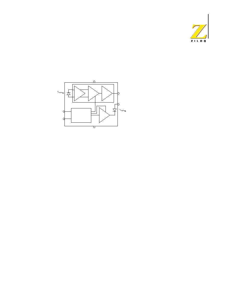
Block Diagram
Figure 1 is the block diagram for the FIR transceiver.
Figure 1. FIR Transceiver Block Diagram
GND
Driver
Driver
Amp
Comp
Mode & Power
Control
V
RXD
SD
TXD
CC
LEDA
ZHX2010
Side-Look FIR Transceiver
PS007009-0302
3
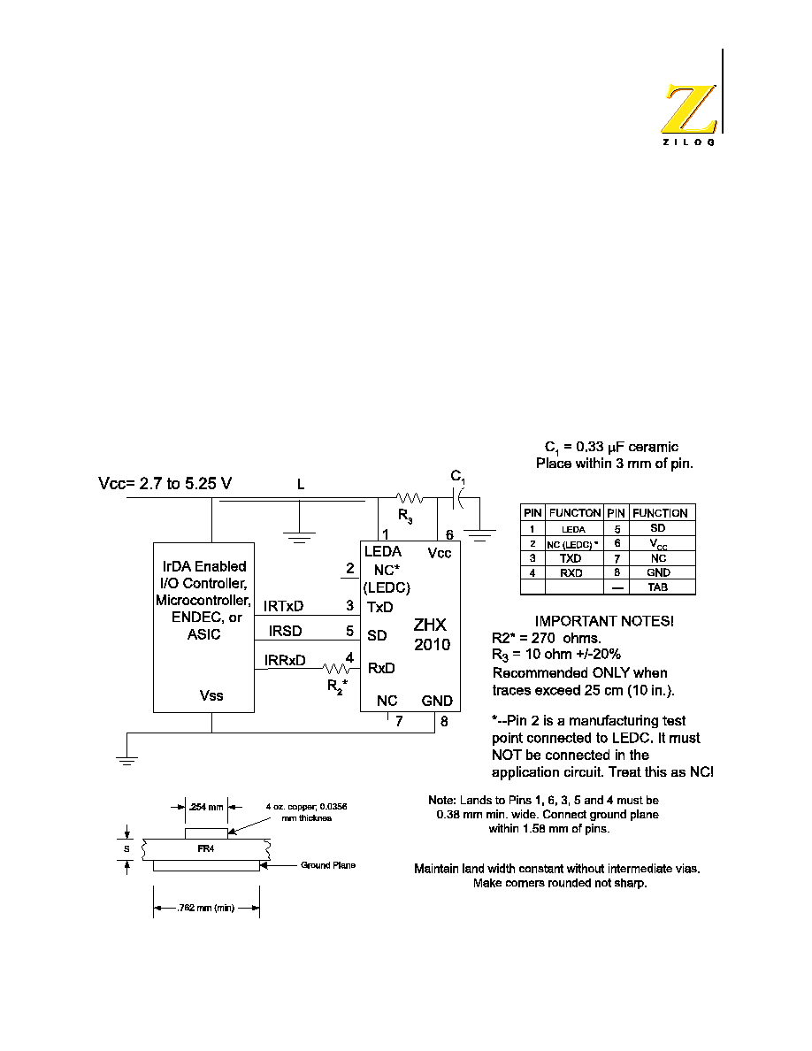
Applications
The ZHX2010 can be used in the following applications:
∑
Notebook PCs
∑
Digital still or video cameras
∑
Portable printers
∑
Cellular telephones
∑
Personal digital assistants
∑
Handheld or battery-operated equipment
Figure 2 shows a typical application of the FIR transceiver.
Figure 2. Application Block Diagram

ZHX2010
Side-Look FIR Transceiver
PS007009-0302
4
Pin Description
Table 1 lists the pin out for the FIR transceiver. The pins are described in this sec-
tion.
V
CC
Positive Supply
(Power)
Connect to positive power supply (2.7≠5.25 V).
Place a 0.33
µ
F, 6 V, +/-20% ceramic bypass capacitor as close as possible to the
V
CC
pin.
GND
(Power)
Connect to ground of the power supply. A solid ground plane is recommended for
proper operation.
TAB
(Shield)
The Shield tab must be soldered to the ground plane.
Table 1. FIR Transceiver Pin Out
Pin
Name
Function
I/O
1
LEDA
IRED anode
--
2
NC(LEDC) Do not connect
--
3
TXD
Transmitter input
I
4
RXD
Receiver output
O
5
SD
Enables shutdown
I
6
V
CC
Supply voltage
--
7
NC
Not connected
--
8
GND
Ground
--
--
TAB
Shield ground
--

ZHX2010
Side-Look FIR Transceiver
PS007009-0302
5
TXD Transmit Data
(Input, active high)
This CMOS input is used to transmit serial data when SD is low. An on-chip
protection circuit disables the IRED driver if the TX pin is asserted for longer than
100
µ
s. When used in conjunction with the SD pin, this pin also provides control
signals to the internal digital serial control interface and legacy mode subsystems.
This input has an internal pull-down resistor that is disabled (open-circuited) dur-
ing shutdown. TXD has integrated digital AC coupling that prevents inadvertent
"always on" IREDs; therefore, no external AC coupling components are required
for input signals between GND and V
CC
.
RXD Receive Data
(Output, active low)
This output indicates received serial data. It is a push-pull CMOS driver capable of
driving a standard CMOS or TTL load. No external pull-up or pull-down resistor is
required.
SD Shutdown
(Input, active high)
This CMOS input pad functions as a shutdown switch and as a mode switch,
allowing bandwidth changes.
Shutdown and Legacy Mode Bandwidth Switching
Assertion of this pin high for a period of time exceeding 500 m places the module
into legacy shutdown mode, reducing current consumption to ~50 nA. On the fall-
ing edge of this signal, the state of the TX pin is sampled and used to set receiver
low bandwidth (TX = Low) or high bandwidth (TX = High) mode.
The transceiver powers on with the upper limit of the receiver bandwidth set to
1.152 Mbits/s operation. To set the bandwidth for operation at 4 Mbits/s, apply the
timings shown in Figure 3 to the SD and the TX inputs.

ZHX2010
Side-Look FIR Transceiver
PS007009-0302
6
Figure 3. Timings for 4 Mbit/s Bandwidth Operation
The internal LED driver is disabled when SD is active and is not
enabled until the next rising edge of TX. This ensures that the
LED is not active during bandwidth adjustment.
It is recommended that the SD pin be connected to GND if the bandwidth adjust-
ment and shutdown modes are not required.
SD
t
s
t
h
TXD
50%
Note:

ZHX2010
Side-Look FIR Transceiver
PS007009-0302
7
Electrical and Timing Specifications
Table 2 through Table 6 list the electrical and timing specifications.
Table 2. Absolute Maximum Ratings
Parameter
Test Conditions Symbol
Min Typical
Max
Unit Comment
Supply voltage
V
CC
≠0.5
5.5
V
Power dissipations
P
D
500
mW
Junction temperature
T
J
125
∞
C
Storage temperature range
Tstg
≠25
85
∞
C
Soldering temperature
20 s at 215
∞
C
215
240
∞
C
Average IRED current
I
LED
(DC)
150
mA
Rep. pulsed IRED current
I
LED
(RP)
600
mA
<90
µ
s, t
on
<25%
Peak IRED current
I
LED
(PK)
1
A
<2
µ
s
TXD input voltage
I
TXD
≠0.5
V
CC
+0.5 V
RXD output voltage
I
RXD
≠0.5
V
CC
+0.5 V
Table 3. Recommended Operating Conditions
Parameter
Symbol
Min
Max
Unit
Supply voltage
V
CC
2.7
5.25
V
Ambient operating temperature
T
amb
≠30
85
∞
C
Table 4. DC Electrical Operating Characteristics
Parameter
Test
Conditions Symbol
Min
Typical
Max
Unit Comment
Supply current, listening
I
CC
1
2.5
3
mA
Supply current, receiving
I
CC
1
5
7
mA No load; no pull-up
resistors
Supply current, shutdown
I
CC
50
100
nA
Specifications hold over the recommended operating conditions unless otherwise noted.
Unspecified test conditions can be anywhere in their operating range. All typical values
are at 25
∞
C
unless otherwise noted.

ZHX2010
Side-Look FIR Transceiver
PS007009-0302
8
Turn-on time
SD-RX
enable
T
on
200
µ
s
Receiver
RX output low voltage
V
OL
0.5
V
Static sink current on RX
2.2 k
load
I
OL
1.2
1.9
mA
RX output high voltage
V
OH
V
CC
≠0.5
V
Static source current on RX
2.2 k
load
I
OH
1.2
1.9
mA
RX edge rates
All data rates t
r
, t
f
20
40
ns
RX resistive load
R
Load
2.2
k
RX capacitive load
C
Load
50
pF
Turnaround time
TAT
200
µ
s
TXD-Min Popt.
RXD
Transmitter
Input voltage low
V
IL
0
0.8
V
TXD, SD
Input voltage high
V
IH
1.4
V
CC
+0.2 V
TXD, SD
Input capacitance
C
i
5
pF
LED optical rise/fall time
LED
t
r
, t
f
40
ns
Integrated
Peak transmit current
I
LED
10
600
mA 25% duty cycle
Average transmit current
I
LED
5
150
mA 25% duty cycle
SIR TX pulse width
T
XPD
1.41
22.13
µ
s
MIR TX pulse width
T
XPD
147
261
ns
FIR TX pulse width
T
XPD
115
135
ns
Table 4. DC Electrical Operating Characteristics (Continued)
Parameter
Test
Conditions Symbol
Min
Typical
Max
Unit Comment
Specifications hold over the recommended operating conditions unless otherwise noted.
Unspecified test conditions can be anywhere in their operating range. All typical values
are at 25
∞
C
unless otherwise noted.

ZHX2010
Side-Look FIR Transceiver
PS007009-0302
9
Table 5. AC Electrical Characteristics
Parameter
Test Conditions
Symbol
Min
Typical
Max
Unit
RX rise time
R=2 k
, C=50 pF
t
r
10
20
40
ns
RX fall time
R=2 k
, C=50 pF
t
f
10
20
40
ns
TX setup to SD high/low
t
s
200
ns
TX hold from SD high/low
t
h
200
ns
RX pulse width
9.6 kbps
t
pw
0.8
20
µ
s
RX pulse width
1.152 Mbps
t
pw
100
800
ns
RX pulse width
4 Mbps, single
t
pw
60
165
ns
RX pulse width
4 Mbps, double
t
pw
185
290
ns
Output delay at 40 mW/cm
2
<1.2 Mbps
t
d
1
2
µ
s
Receiver latency
t
L
100
µ
s
RX valid after shutdown
t
RXDEN
60
µ
s
LED protection timeout
t
LEDP
100
µ
s
Table 6. Optical Characteristics
Parameter
Test Conditions
Symbol
Min
Typical
Max
Unit
Minimum detection irradiance
SIR: 9.6≠115 kbps
E
MIN
2
3
µ
W/cm
2
MIR: 1.152 Mbps
E
MIN
2.5
4
µ
W/cm
2
FIR: 4 Mbps
E
MIN
7
µ
W/cm
2
Output radiant intensity
I
E
100
140
320
mW/sr
Peak wavelength
I
P
860
900
nm
Optical overshoot
25
%

ZHX2010
Side-Look FIR Transceiver
PS007009-0302
10
Transceiver Performance
Figure 4 through Figure 6 show the performance of the FIR transceiver.
Figure 4. Typical Ie Versus Angle
Figure 5. Typical SIR Ee Versus Angle

ZHX2010
Side-Look FIR Transceiver
PS007009-0302
11
Figure 6. Typical FIR Ee Versus Angle

ZHX2010
Side-Look FIR Transceiver
PS007009-0302
12
Mechanical Specifications
Figure 7 shows the mechanical specifications for the FIR transceiver.
The ZiLOG ZHX2010 transceiver will continue to be marked as
the original Calibre part number, CHX2010.
Figure 7. ZHX2010 Mechanical Specifications
Note:

ZHX2010
Side-Look FIR Transceiver
PS007009-0302
13
Soldering and Cleaning Recommendations
Follow these recommendations to maintain the performance of the ZHX2010
transceiver.
Reflow Soldering
∑
Reflow soldering paste is recommended:
Melting temperature: 178 ∞C ~ 192 ∞C
Composition: Sn 63%, Pb 37%
∑
The recommended thickness of the metal mask is between 0.2 mm and
0.25 mm for screen printing.
∑
Number of soldering times: 2 times maximum
∑
The temperature profile at the top surface of ZHX2010, shown in Figure 8, is
recommended.
Figure 8. Temperature Profile for the Top Surface
Manual Soldering
∑
Use 63/37 or silver solder.
∑
Use a soldering iron of 25 W or smaller. Adjust the temperature of the
soldering iron below 300 ∞C.
∑
Finish soldering within 3 seconds.
∑
Handle only after the ZHX2010 has cooled off.
10 sec Max.
40 sec Max.
230 C Max.
60 ~ 120 sec
140 C ~ 160 C
4 C/sec Max.
250
200
150
100
4 C/sec Max.
T
emper
ature
(deg
rees C)
Time

ZHX2010
Side-Look FIR Transceiver
PS007009-0302
14
Cleaning
Perform cleaning after soldering under the following conditions:
∑
Cleaning agent: Alcohol
∑
Temperature and time: 30 seconds below 50 ∞C or 3 minutes below 30 ∞C
∑
Ultrasonic cleaning: Below 20 W

ZHX2010
Side-Look FIR Transceiver
PS007009-0302
15
Packing, Storing, and Baking Recommendations
Follow these recommendations to maintain the performance of the ZHX2010
transceiver.
Storage
To avoid moisture absorption, ZHX2010 reels must remain in the original,
unopened moisture-proof packing. Parts must be soldered within 48 hours after
unpacking. Reels that have been unpacked, but will not be soldered within 48
hours, must be stored in a desiccator.
Baking
Parts that have been stored over 12 months or unpacked over 48 hours must be
baked under the following guidelines.
Reels
60 ∞C for 48 hours or more
Loose Parts
∑
100 ∞C for 4 hours or more
or
∑
125 ∞C for 2 hours or more
or
∑
150 ∞C for 1 hour or more

ZHX2010
Side-Look FIR Transceiver
PS007009-0302
16
Moisture-Proof Packing
In order to avoid moisture absorption during transportation and storage, ZHX2010
reels are packed in aluminum envelopes (see Figure 9) that contain a desiccant
with a humidity indicator. The indicator changes color from blue to pink as mois-
ture is absorbed.
Figure 9. FIR Transceiver Packaging
ZHX2010
Side-Look FIR Transceiver
PS007009-0302
17
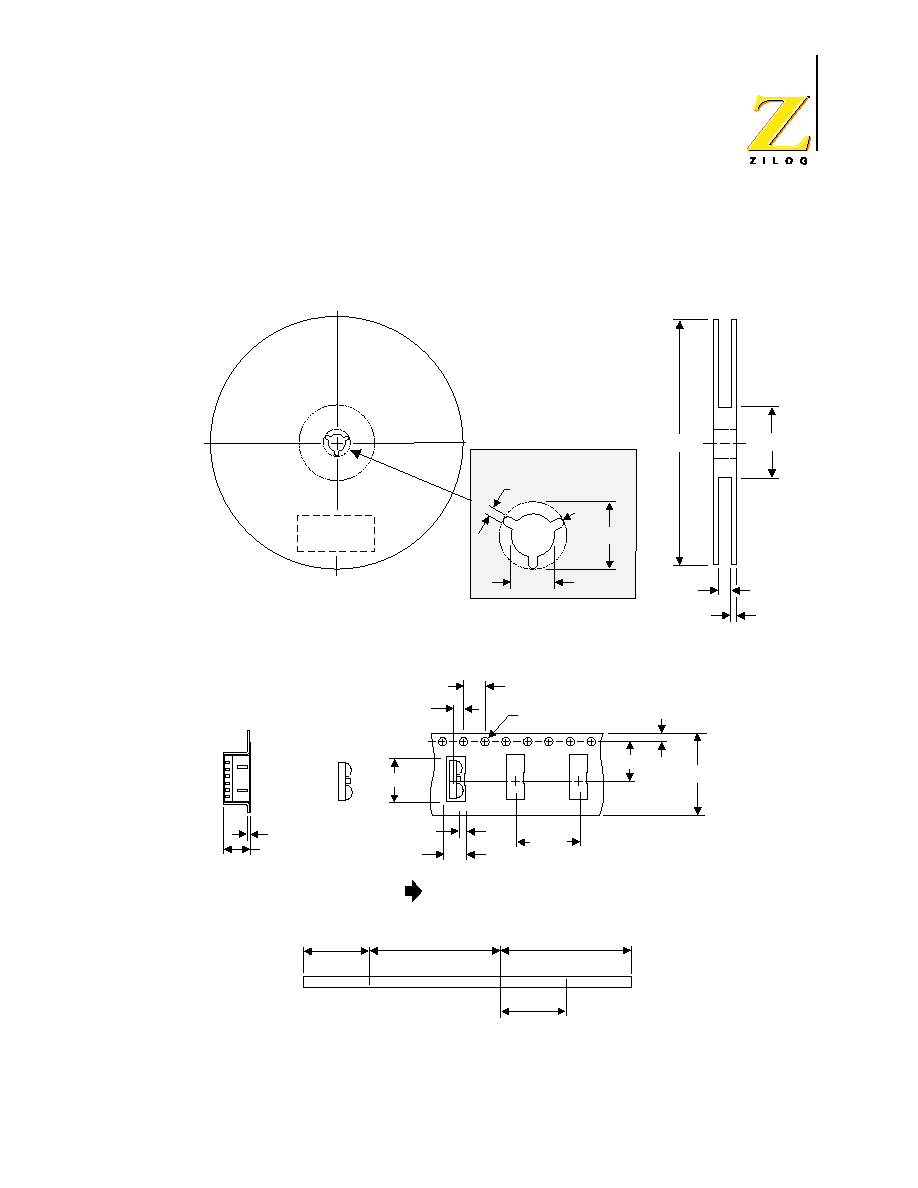
Taping Specifications (in accordance with JIS C 0806)
Figure 10 shows the reel dimensions, and Figure 11 shows the tape dimensions
and configuration.
Figure 10. Reel Dimensions
Figure 11. Tape Dimensions and Configuration
LABEL
PASTED
HERE
80 ± 1 DIA.
2 ± 0.5
17.5
+ 2.0
- 0.0
330 DIA.
2.0 ± 0.5
13.0 ± 0.5
21.0 ± 0.8
R 1.0
DETAIL
(Unit:mm)
0.4 ± 0.05
1.5 DIA.
+ 0.1
- 0.0
4.4 ± 0.1
ANODE
V
SS
16 ± 0.3
PULL OUT DIRECTION
7.5 ± 0.1
1.75 ± 0.1
1.4 ± 0.1
5.24 ± 0.1
.73 ± 0.1
4 ± 0.1
10.2 ± 0.1
PARTS MOUNTED
LEADER
EMPTY
(40 mm MIN)
(400 mm MIN)
EMPTY
(40 mm MIN)
QUANTITY
2,000 Pieces per reel
(Unit:mm)
8.0 ± 0.1

ZHX2010
Side-Look FIR Transceiver
PS007009-0302
18
Customer Feedback Form
If you experience any problems while operating this product, or if you note any inaccura-
cies while reading this product specification, please copy and complete this form, then
mail or fax it to ZiLOG (see Return Information, below). We also welcome your sugges-
tions!
Customer Information
Product Information
Return Information
ZiLOG
System Test/Customer Support
532 Race Street
San Jose, CA 95126-3432
Fax: (408) 558-8300
Email: tools@zilog.com
Problem Description or Suggestion
Provide a complete description of the problem or your suggestion. If you are reporting a
specific problem, include all steps leading up to the occurrence of the problem. Attach
additional pages as necessary.
_______________________________________________________________________________
_______________________________________________________________________________
_______________________________________________________________________________
_______________________________________________________________________________
Name
Country
Company
Phone
Address
Fax
City/State/Zip
email
Serial # or Board Fab #/Rev #
Software Version
Document Number
Host Computer Description/Type