Preliminary Datasheet, February 11th 2002 1/17
ZMD30010
LIN-Transceiver
Features
p data rate up to 20 kBaud
p operation voltage from 6.5 to
18 V DC
p low standby current
consumption
p very low electromagnetic
emission
p high electromagnetic
immunity
p low power consumption
in recessive state
p local and remote wake-up
function
p slew rate control enables
low radio frequency
interferences
p ±4kV ESD protection on
LIN-, WAKE-, VSUP- and
GND-pin
p protection against thermal
overload, short circuit and
load dump
As an additional capability the
ZMD30010 enables to control
an external voltage regulator
which supplies other devices.
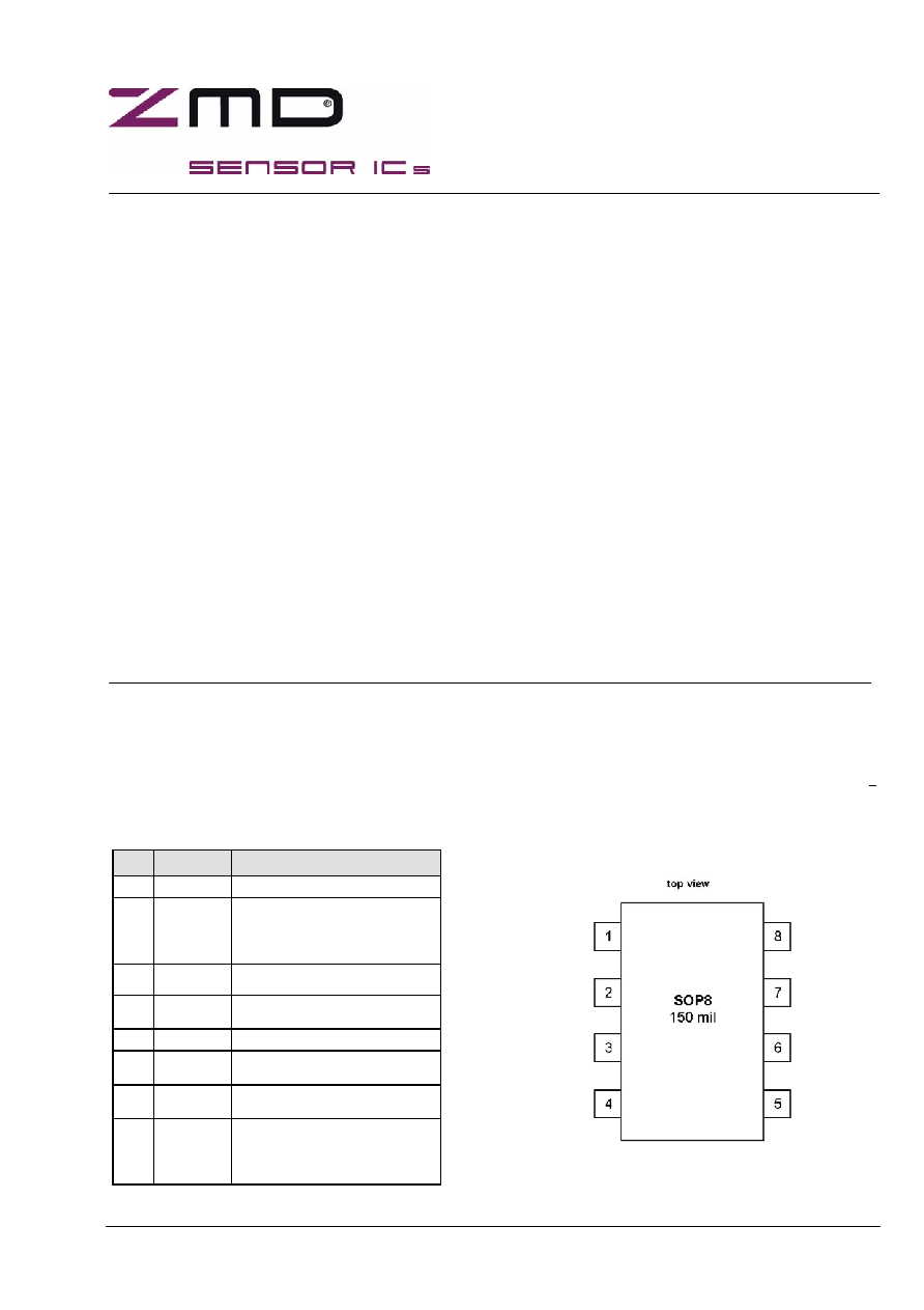
Pin Configuration and Description
PIN Symbol
Description
1
RXD
receive data output
2
EN
sleep control input
normal mode=high
sleep mode=low
3
WAKE
local wake-up input
4
TXD
transmit data input
5
GND
ground
6
LIN
single wire bus input/output
7
VSUP
battery supply input
8
INH
battery related inhibit output
to control an external
voltage regulator
Description
The LIN Transceiver ZMD30010 is
an integrated circuit realised in
CMOS technology and packed into a
SOP 8 case.
The device works as an interface
between a protocol controller and
the physical bus in a Local
Interconnect Network.
The functionality corresponds to the
"LIN Specification Rev. 1.2".
The ZMD30010 is especially suitable
to drive the bus line in automotive
and industrial applications.
Therefore it is designed to withstand
the particular conditions of an
automotive environment.
The device has an internal voltage
regulator to supply itself.
It is also equipped with a sleep mode
and a wake-up-function in order to
reduce current consumption.
Ordering Information
Device
Operation Temperature Range
Package
ZMD30010AF
-40∞C . . . 125∞C
SOP8
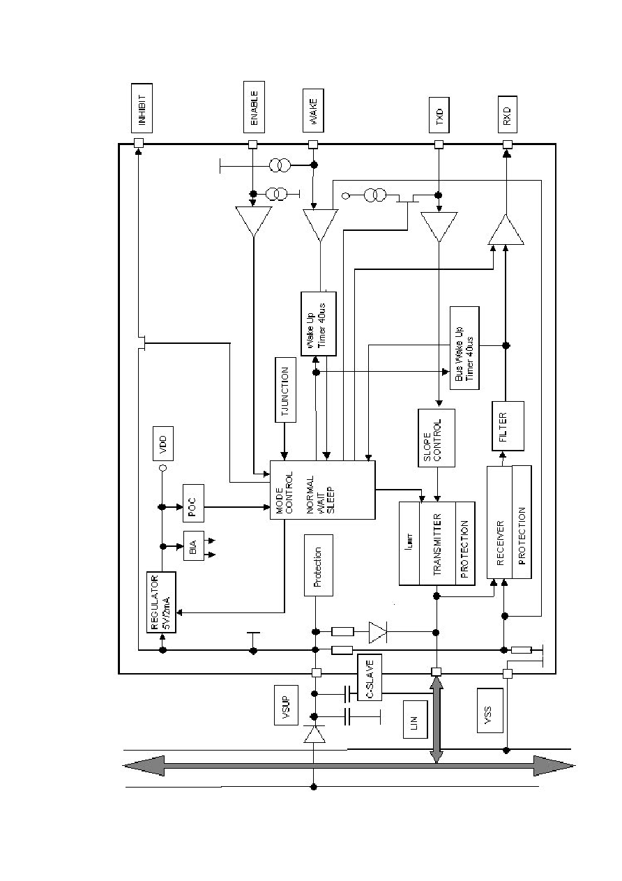
Figure 1: Block Diagram
Preliminary Datasheet, February 11th 2002 3/17
ZMD30010
LIN-Transceiver
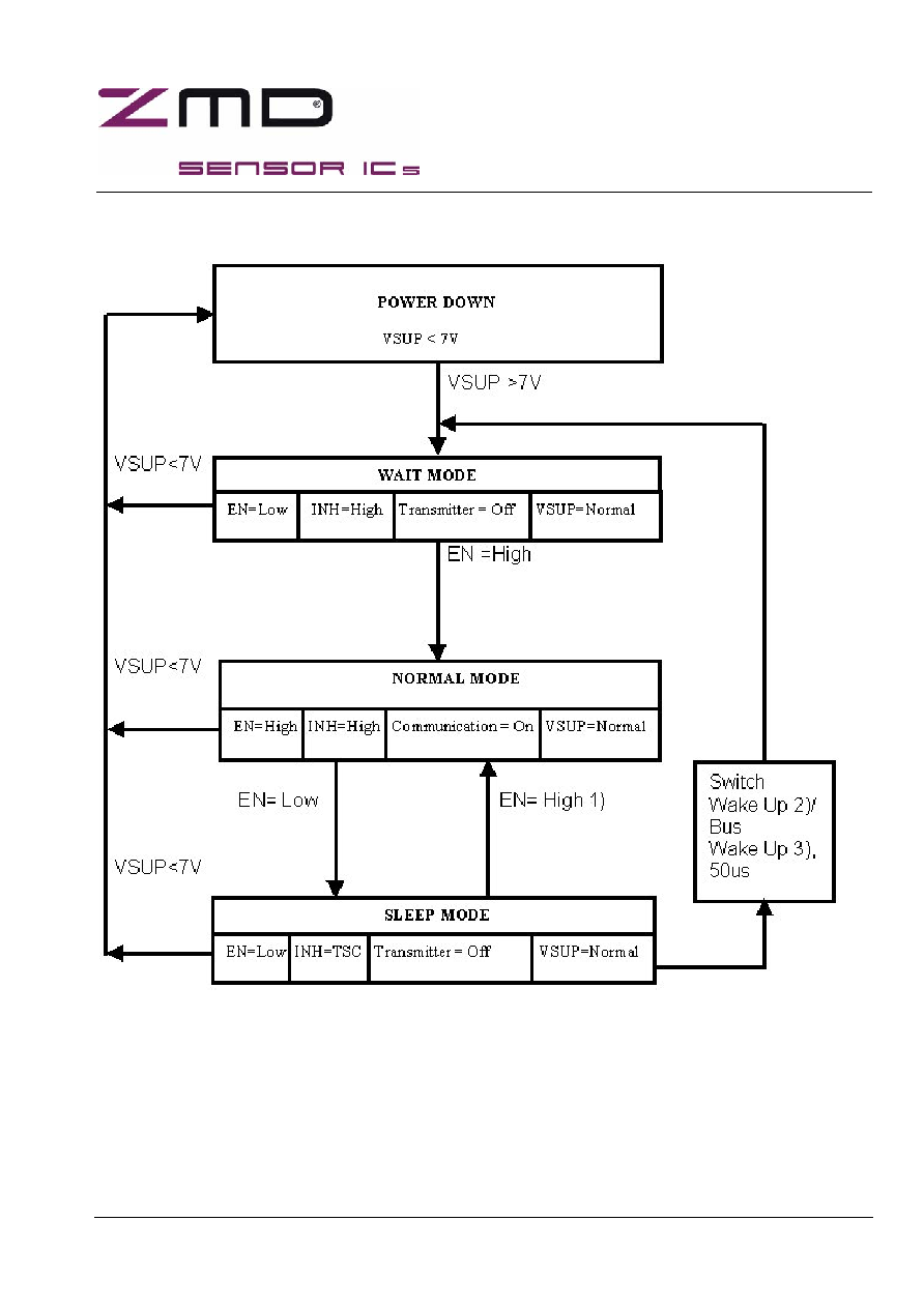
Figure 2: State Machine
Wake Up Events:
1) Internal Node Activity
2) Wake Switch
3) LIN-Bus Wake Up
TSC: three state current

Preliminary Datasheet, February 11th 2002 4/17
ZMD30010
LIN-Transceiver
Figure 3: Flow Diagram State Machine
TR = transmitter, EN = enable, INH = inhibition, WU = wake-up, TJ=Tjunction
Preliminary Datasheet, February 11th 2002 5/17
ZMD30010
LIN-Transceiver
Functional Description
Supply Voltage VSUP
The VSUP-pin has to be protected by an external diode against pole interchange of the battery
supply. The protection against galvanic and capacitive coupled transients is realised by a special
internal circuitry combined with the external capacitances C
SUP
, C
LIN
and C
SLAVE
.
The nominal supply voltage is between 6.5 and 18 V DC. A voltage control prevents an incorrect bus
transfer below the operating voltage range.
The quiescent current in the sleep-mode amounts to appr. 25 µA. In the normal-mode the quiescent
current amounts to max. 2 mA in the state of dominant LIN-bus.
VSS-PIN
The VSS-pin represents the ground level. Level suspensions 2.5 V don't influence the data transfer.
A ground loss in the recessive state does not lead to a significant current at the LIN-pin.
LIN-Bus-Pin
The modules receiver and transmitter realise the bidirectional LIN-bus-connection.
Receiver:
The input voltage of the receiver depends on the supply voltage ratiometricly. The threshold amounts
to 0.4 respective 0.6 VSUP with a hysteresis of < 10 % VSUP. The receiver is active in the sleep
mode too. The filter in the input signal path suppresses spikes with a duration of <± 4 µs.
Transmitter:
The transmitter consists of a low-side-driver supplying 40 mA at a output-voltage of 1.2 V.
It transmits a low level if there is a low level on the TXD-pin. An internal pull-up resistor of 30 k
pushes the bus node to the high level in the locked transmitter state.
A diode which is switched in-line to the resistor prevents a reflow current from the bus into the battery
supply line in the case of a local supply loss or a ground level suspension.
The transmitter is only active in the normal-mode. In the sleep-mode and in the wait-mode the
transmitter is tristated.
In the case of short circuits to battery supply or to ground the drivers current limitation begins to work
at 90 mA typically. The driver is also protected against thermal overloads.
In the range from -18 V to 30 V the current VSUP-LIN is determined only by the pull-up-resistor. The
in-line-switched diode prevents a current from the LIN-pin to the VSUP-pin.
A VSUP loss in the recessive driver state does not lead to a significant current at the LIN-pin.
A slope-control adjusts both edges (falling edge from the recessive to the dominant driver state and
rising edge from the dominant to the recessive driver state) to 2V/µs typically. As a result the
electromagnetic emission is minimal.
The capacitive LIN-bus-load has to be restricted to a total <10 nF at a total resistance <1 k. This is
done to ensure the symmetry of both edges.