 | –≠–ª–µ–∫—Ç—Ä–æ–Ω–Ω—ã–π –∫–æ–º–ø–æ–Ω–µ–Ω—Ç: ZMD44101 | –°–∫–∞—á–∞—Ç—å:  PDF PDF  ZIP ZIP |
ZMD44101
Single-Chip 868MHz to 928MHz RF Transceiver
Introduction
Key Features
Description
Copyright © 2005, ZMD AG
Data Sheet - March 2005
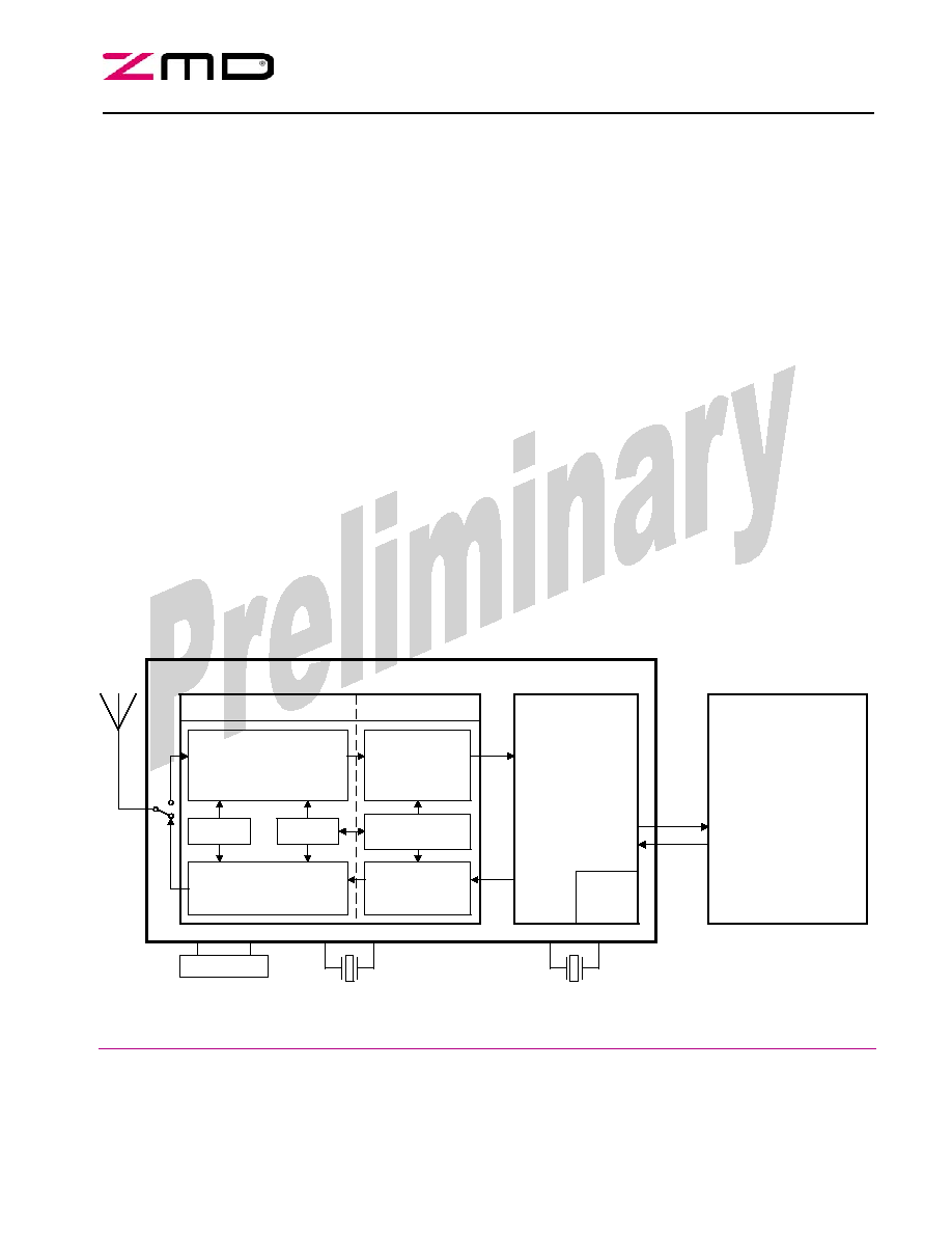
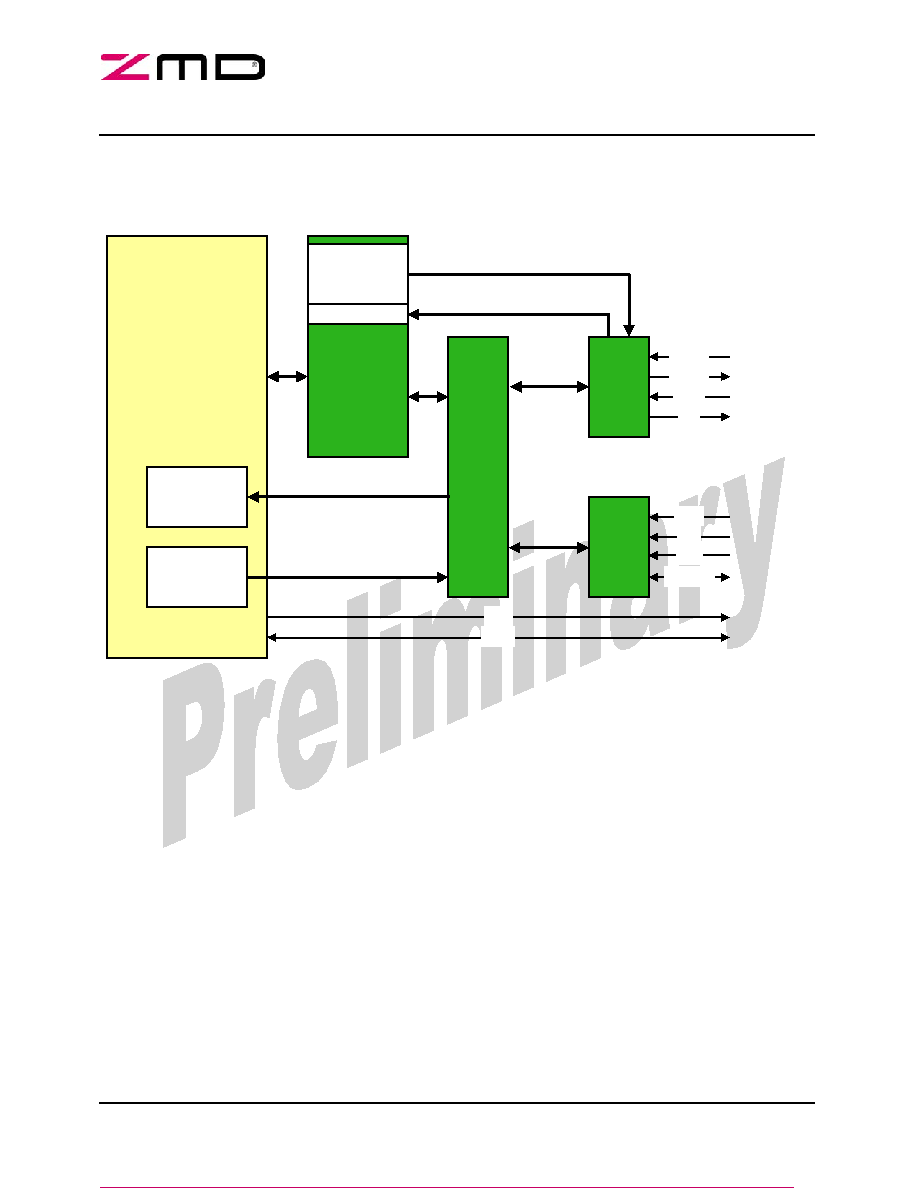
The ZMD44101 is a fully integrated system-on-chip
CMOS transceiver, providing license free multi-
channel operation in the 868.3MHz (EU) and
902MHz to 928MHz (US) ISM bands. The low
power baseband transceiver is optimized for data
rates up to 40kbp/s and incorporates direct
sequence spread spectrum technology to assure
reliable data transfer in hostile RF environments.
The high level of integration, shown below,
includes a thin Media Access Controller, resulting
in a minimum of external components and lower
application costs.
IEEE 802.15.4 compliant
ISM band transceiver with RF and
baseband
Direct Sequence Spread Spectrum (DSSS)
Burst data rate 20kbit/s (EU), 40kbit/s (US)
Transmit range up to 100 meter (LoS)
Low power for battery operated devices
SPI and Parallel interfaces
Compliant PHY and Thin MAC
Available in 48-lead QFN (7mm X 7mm)
package
Applications
Operating Reference Data
Energy Management
Temperature Range................-40∞C to +85∞C
Remote Metering and Control
Supply Voltage, V
DD
............................+2.4 V
Home and Building Control
Typical Supply Current (Tx active)...........32mA
Industrial Networks
Typical Supply Current (Rx active)...........28mA
Remote Keyless Entry (two-way)
Typical Supply Current (sleep mode)...........2µA
Health Monitor Networking
Frequency Range.............868MHz to 928MHz
Airframing
Error detection (CRC)
Duty Cycle
Host Interface
Thin HW-MAC
Complete PHY
Analog
Digital
Analog Receiver
PLL
Analog Transmitter
Digital RX
1) Synchronization
2) Despreading
3) Demodulation
4) Digital Filtering
Digital TX
1) Spreading
2) Pulse Shaping
Dedicated DSP
Functions
Additional MAC functions
Protocol implementation
Network support
Upper layer functionality
Application
Interfaces (sensor)
Application Specific
Controller/Sensor
SPI or
parallel
Registers
ZMD 44101
24MHz
32.768kHz
PLL RC-LPF
Power
Manager
All rights reserved. The material contained herein may not be reproduced, adapted, merged, translated, stored, or used without the prior
written consent of the copyright owner. The information furnished in this publication is preliminary and subject to changes without notice.

ZMD44101
Single-Chip 868MHz to 928MHz RF Transceiver
PRELIMINARY - March 2005
Information is current as of publication date. Products conform to specification per the terms of the ZMD standard warranty.
Production testing does not necessarily include testing of all parameters. Copyright © 2004, ZMD AG
Table of Contents
1
Pin Diagram .................................................................................................................................... 3
2
General Device Specifications........................................................................................................ 4
2.1
Absolute Maximum Ratings ................................................................................................... 4
2.2
Recommended Operating Conditions .................................................................................... 4
2.3
D.C. Electrical Characteristics................................................................................................ 4
2.4
Digital I/O................................................................................................................................ 5
3
A.C. Electrical Characteristics ........................................................................................................ 5
3.1
General................................................................................................................................... 5
3.2
Startup time ............................................................................................................................ 5
4
Interfaces ........................................................................................................................................ 6
4.1
Overview ................................................................................................................................ 6
4.2
Serial Peripheral Interface (SPI) ............................................................................................ 7
4.2.1
SPI Configuration............................................................................................................... 7
4.3
Parallel Interface .................................................................................................................... 9
5
Registers....................................................................................................................................... 10
5.1
MAC control + status register............................................................................................... 10
5.2
MAC timing registers............................................................................................................ 11
5.3
Other MAC registers............................................................................................................. 12
5.4
MAC header registers .......................................................................................................... 13
5.5
PHY registers ....................................................................................................................... 13
6
Application circuit ≠ external components .................................................................................... 14
7
ZMD44101 System Performance Summary................................................................................. 15
8
System Description ....................................................................................................................... 16
8.1
General Block Diagram ........................................................................................................ 16
8.2
Receiver Chain..................................................................................................................... 17
8.2.1
RAGCL - AGC Level Register ......................................................................................... 18
8.3
Transmitter Chain................................................................................................................. 18
8.3.1
RTXM - Transmitter Mode Register................................................................................. 18
8.4
RF Phase Locked Loop........................................................................................................ 19
8.5
Reference Crystal Oscillator (24MHz).................................................................................. 20
8.6
Low Power Crystal Oscillator (32.768kHz)........................................................................... 21
8.7
CLKO - Clock Output Configuration ..................................................................................... 21
8.8
Power Management ............................................................................................................. 22
9
Mechanical Specifications............................................................................................................. 23
9.1
Package ............................................................................................................................... 23
10
List of abbreviations ...................................................................................................................... 25
11
References.................................................................................................................................... 25
ZMD44101
Single-Chip 868MHz to 928MHz RF Transceiver
PRELIMINARY
-
March 2005
Page 3 of 26
Copyright © 2005, ZMD AG
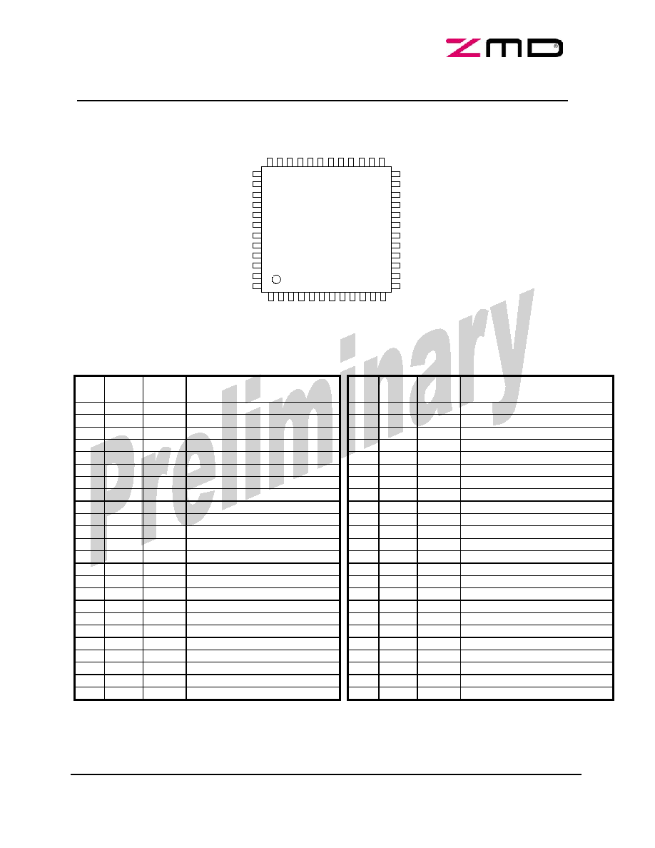
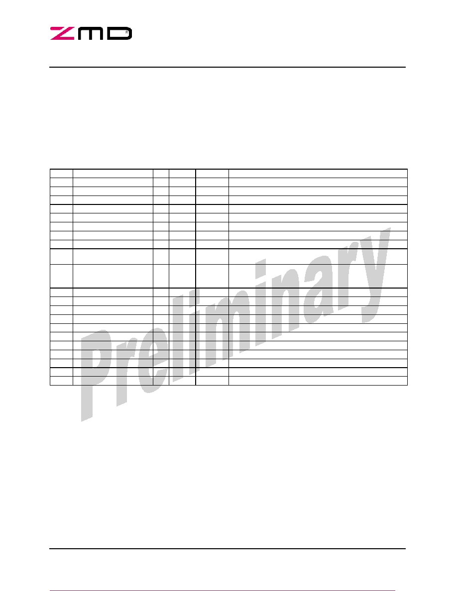
1 Pin
Diagram
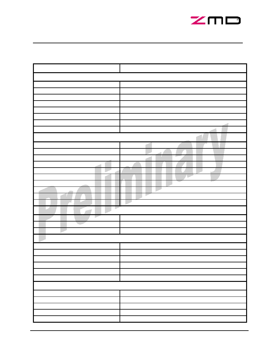
Figure 1.1 provides the pin layout for the ZMD44101 and Table 1.1 the description of the respective pins.
ZMD44101
48 QFN (=MLF)
TOP VIEW
1
48
12
13
24
25
36
37
WR
RD
DVDD_3.3
DVSS
DVDD
ALE
AVDD
AVSS
RTC1
RTC2
NC
NC
SS
IRQ
GPD
DVDD_3.3
DVDD
RSN
DVDD
NC
NC
AVDD
LPF2
LPF1
MO
S
I
MI
S
O
SCK
DA
[
0
]
DA
[
1
]
DA
[
2
]
DA
[
3
]
DA
[
4
]
DA
[
5
]
DA
[
6
]
DA
[
7
]
CL
KO
XT
AL
2
XT
AL
1
AV
D
D
RFO
A
VSS
RFIO
A
VSS
AV
D
D
A
VSS
AV
D
D
NC
NC
Figure 1.1 - Pin Layout
Pin
No.
Pin
Name
Pin
Type
Description
Pin
No.
Pin
Name
Pin
Type
Description
1
NC
-
No connection
25
MOSI
CMOS IO
SPI interface - master out, slave in
2
NC
-
No connection
26
MISO
CMOS IO
SPI interface - master in, slave out
3
AVDD
AVDD
Analog power supply
27
SCK
CMOS IO
SPI interface - serial clock
4
AVSS
Ground
Analog ground
28
DA0
CMOS IO
Data address
5
AVDD
AVDD
RF power supply
29
DA1
CMOS IO
Data address
6
AVSS
Ground
RF ground
30
DA2
CMOS IO
Data address
7
RFIO
RF IO
RF receiver input and transmitter output
31
DA3
CMOS IO
Data address
8
AVSS
Ground
RF ground
32
DA4
CMOS IO
Data address
9
RFO
RF Output
RF transmitter output
33
DA5
CMOS IO
Data address
10
AVDD
AVDD
Analog PLL power supply
34
DA6
CMOS IO
Data address
11
XTAL1
Analog Input 24MHz crystal oscillator input
35
DA7
CMOS IO
Data address
12
XTAL2
Analog Output 24MHz crystal oscillator output
36
CLKO
CMOS Output Clock (to external device)
13 LPF1
Analog
Output
Loop filter, charge-pump node
37
WR
CMOS IO
Write data address
14 LPF2
Analog
Input
Loop filter, VCO tune node
38
RD
CMOS IO
Read data address
15
AVDD
AVDD
Analog PLL VCO power supply
39
DVDD_3.3 DVDD_3.3
Digital IO 3.3V power supply (post-driver)
16
NC
-
No connection
40
DVSS
Ground
Digital ground
17 NC
-
No
connection
41
DVDD
DVDD
Digital core 2.4V power supply (core and pre-driver)
18
DVDD
DVDD
Digital PLL power supply
42
ALE
CMOS IO
Address latch enable
19
RSN
CMOS Input Asynchronous chip reset (low - active)
43
AVDD
AVDD
Analog power supply
20
DVDD
DVDD
Digital core 2.4V power supply (core and pre-driver)
44
AVSS
Ground
Analog ground
21
DVDD_3.3 DVDD_3.3
Digital IO 3.3V power supply (post-driver)
45
RTC1
Analog Input 32.768kHz crystal oscillator input
22
GPD
CMOS IO
Global Power Down (from external device)(h-active)
46
RTC2
Analog Output 32.768kHz crystal oscillator output
23
IRQ
CMOS Output Interrupt (to external device)(low active)
47
NC
-
No Connection
24
SS
CMOS IO
SPI interface - slave select
48
NC
-
No Connection
Table 1.1 - Pin Descriptions
ZMD44101
Single-Chip 868MHz to 928MHz RF Transceiver
P
RELIMINARY - March 2005
Copyright © 2005, ZMD AG
Page 4 of 26
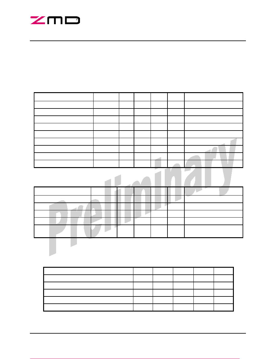
2 General Device Specifications
Electrical characteristics over full range of operating conditions, typical values are AVDD, DVDD = 2.4V,
DVDD_3.3 = 3.3 V, T
a
= 25
∞C, unless otherwise noted.
2.1 Absolute
Maximum
Ratings
Caution: Operation beyond these values may cause permanent damage to the device or decrease in
reliability. Note: Values are over free-air temperature unless otherwise noted.
Parameter Symbol
Min
Typ
Max
Unit Notes
Analog Supply Voltage
AVDD
-
-
3.5
V
Digital Supply Voltage
DVDD
-
-
3.5
V
Digital IO Supply Voltage
DVDD_3.3
-
-
4.6
V
Input Voltage
V
i
-
-
6
V
at CMOS IO
Output Voltage
V
o
-
-
4.6
V
at CMOS IO
Analog Input Voltage
V
ana
-
-
3.5
V
at analog IO
Input RF Level
P
in
-
-
20
dBm
Storage Temperature
T
strg
-65 - 150
∞C
ESD Protection
V
esd
-
-
2
kV
HBM (100pF, 1.5k)
2.2 Recommended Operating Conditions
Parameter Symbol
Min
Typ
Max
Unit Notes
Analog Supply Voltage
AVDD
2.2
2.4
2.7
V
Digital Supply Voltage
DVDD
2.2
2.4
2.7
V
Digital IO Supply Voltage
DVDD_3.3
3.0
3.3
3.6
V
Ambient Temperature
T
a
-40
+27
+85
∞C
Industrial
range
Frequency of Operation
f
op
860 930
MHz
868.3MHz (EU), 902MHz
to 928MHz (US)
2.3 D.C.
Electrical Characteristics
Note: Values are for supply current.
Parameter Symbol
Min
Typ
Max
Unit
Sleep mode (32kHz crystal and timer on)
Idd
-
2
-
µA
Idle mode (24MHz crystal on)
Idd
-
1
-
mA
Transmit
mode
Idd - 32 -
mA
Receive mode, synchronization
Idd
-
31
-
mA
Receive mode, normal
Idd
-
28
-
mA
ZMD44101
Single-Chip 868MHz to 928MHz RF Transceiver
PRELIMINARY
-
March 2005
Page 5 of 26
Copyright © 2005, ZMD AG
2.4 Digital I/O
Module Symbol
Min
Typ
Max
Unit
Notes
CMOS Input V
IL
-0.3
0.8
V
V
IH
2
5.5
V
CMOS Output
V
OL
0.4
V
V
OH
2.4 V
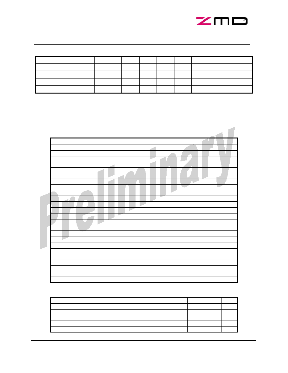
3 A.C. Electrical Characteristics
Electrical characteristics over full range of operating conditions, typical values are AVDD, DVDD = 2.4V,
DVDD_3.3 = 3.3 V, TA = 25
∞C, unless otherwise noted.
3.1 General
Symbol Min Typ
Max Unit
Note
Transmitter
P
out
-3
0
3
dBm
output power at 50
P
low1
-7
dBm
low output power mode 1
P
low2
-14
dBm
low output power mode 2
P
low3
-21
dBm
low output power mode 3
P
SL
-30
dBm
max. spurious emission=1
st
side lobe
Harmonics -35
dBm
P
N
-57
dBm
Standby
radiation
r
EU
300
kBit/s Chip rate (EU) @ channel 0
r
US
600
kBit/s Chip rate (US) @ channel 1 to 10
Receiver
P
min
-100
dBm
at packet error rate (PER) <1%
NF
10 dB
P
in,max
-20
dBm
maximum usable input power
IIP3
-20 dBm
IIP2
25 dBm
LO leakage
-57
dBm
PLL
bandwidth 860 930 MHz
f
ref
24
MHz
crystal with 32pF C
load
=32pF
BW
LPF
300
kHz
LPF
bandwidth
f
res
732
Hz
frequency
resolution
f
cs
2
MHz
channel spacing for IEEE 802.15.4
N
-85
dBc
(10...100) kHz offset
3.2 Startup
time
Parameter Time
Unit
Power on to idle mode
1.0 (typical)
ms
Idle mode to Transmitter ready
0.18
ms
Idle mode to Receiver ready
0.2
ms
Receiver to Transmitter turnaround
0.2
ms
Transmitter to Receiver turnaround
0.2
ms
ZMD44101
Single-Chip 868MHz to 928MHz RF Transceiver
P
RELIMINARY - March 2005
Copyright © 2005, ZMD AG
Page 6 of 26
Digital Core
TX FIFO
128x8
RX FIFO
256x8
Inter-
face
SPI
Paral-
lel
Reg.
Bank
MISO
MOSI
SCK
SS
ALE
RD
WR
DA[7:0]
IRQ
GPD
SPIconfig[5:0]
SPItx[7:0]
SPIstart
SPIrx[7:0]
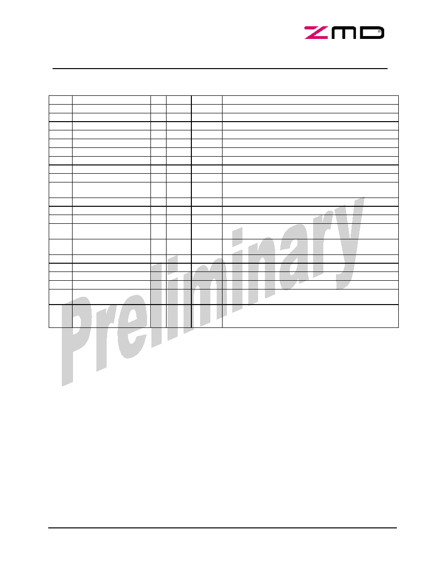
4 Interfaces
4.1 Overview
Figure 4-1: Interface Block Diagram
The ZMD44101 provides a parallel interface and an SPI to access the internal register bank, the TX and
the RX FIFO. Additionally it has a IRQ output and a dedicated global power down (GPD) input.
By default both interfaces the parallel and the SPI as slave are available. For proper operation the unused
interface shall be disabled. The parallel interface is disabled by setting RD,WR, and ALE to high, putting
the DataAddress[7:0] bus into High-Z state. The SPI is disabled by setting SS to high.
The SPI can also be configured as master. In the master setup is behaves like a remote interface
which can be controlled by the external microcontroller via the ZMD44101 parallel interface and some SPI
control register in the register bank.
ZMD44101
Single-Chip 868MHz to 928MHz RF Transceiver
PRELIMINARY
-
March 2005
Page 7 of 26
Copyright © 2005, ZMD AG
4.2 Serial Peripheral Interface (SPI)
4.2.1 SPI
Configuration
The SPI is configured via the SPIconfig (R/W ) register.
A standard based SPI is used by default in slave mode. Certain registers can switch the interface to
master mode to work with another slave. In that case the parallel microcontroller interface is used to
control the ZMD44101. The interface provides the standard lines MISO, MOSI, SCK and SS. For Write
Access the first bit of the first byte on MOSI has to be `0'. For Read Access the first bit of the first byte
written to MOSI has to be `1'. SS (Slave Select) has to be `0' when accessing the ZMD44101 through the
SPI.
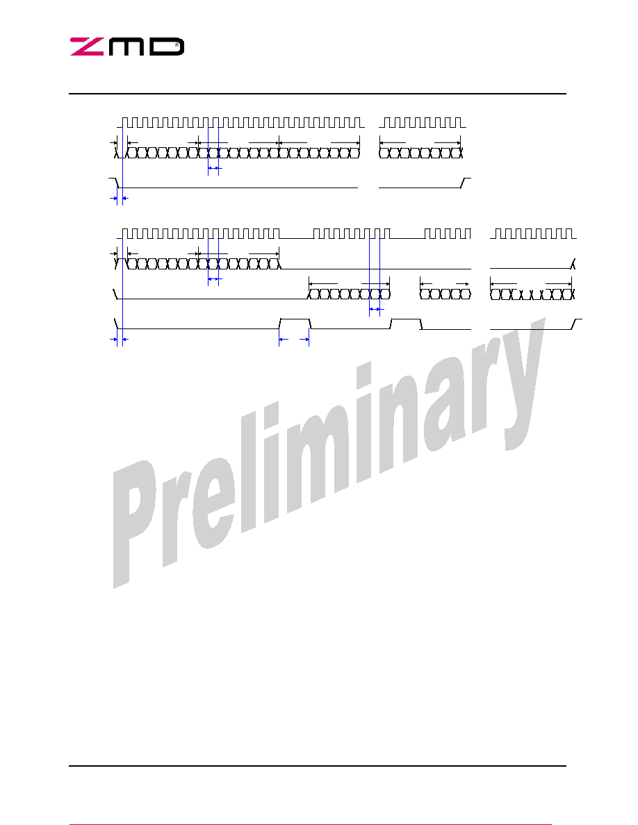
The ZMD44101 uses a data transfer protocol allowing single and multiple byte read/write access.
All bytes are transmitted with the MSB first and the LSB last.
The protocol always starts by writing 2 bytes to the SPI slave via the MOSI line. The MSB of the first byte
is the read/write indicator. A high bit stands for read access and a low bit for write access. The read/write
bit is followed by the length[6:0] descriptor N. It controls the length of the data frame D
0
[7:0] to D
N-1
[7:0]. N
hast to be in a range 1 to 127.The second byte is the address[7:0]. For TX/RX FIFO access the address
are 0x80 and 0x81 respectively. Note that the TX FIFO only allows write access and the RX FIFO read
access. In the case of register bank access a number of N bytes is read starting from address[7:0] up to
address[7:0]+(N-1). In the case the FIFO locations 0x80 or 0x81 are within this range they are skipped
and the read/write access is continued at location 0x82.
For write access the address[7:0] byte is followed by the data frame D
0
[7:0] to D
N-1
[7:0]. In figure 4-2
the slave select signal SS is low during the complete write transfer. However it is also allowed to insert SS
high gaps between each byte.
In the read access protocol the data frame is shifted out by the slave on the MISO line. Before each data
byte a SS high gap is required. Similar to the write access a SS high gap can be inserted before the
address[7:0] byte.
Timing parameters are listed in the following table.
US mode
EU mode
Parameter Description
min
max
min
max
tcp
SCK clock period
0.50 µs 1.00
µs
tsc
SS low to SCK active edge
0.25 µs 0.50
µs
tss
SS high pulse with
1.00 µs 2.00
µs
ZMD44101
Single-Chip 868MHz to 928MHz RF Transceiver
P
RELIMINARY - March 2005
Copyright © 2005, ZMD AG
Page 8 of 26
D
N-1
[7:0]
D
1
[7:0]
D
0
[7:0]
Length[6:0] (N)
A[7:0]
D
0
[7:0]
SS
MOSI
MISO
...
...
tss
write access:
read access:
W
SCK
SCK
Length[6:0] (N)
A[7:0]
MOSI
R
SS
D
N-1
[7:0]
...
tsc
tsc
tcp
tcp
tcp
Figure 4-2: Transfer Protocol (SPI Slave Mode), CPHA=0 CPOL=0
ZMD44101
Single-Chip 868MHz to 928MHz RF Transceiver
PRELIMINARY
-
March 2005
Page 9 of 26
Copyright © 2005, ZMD AG
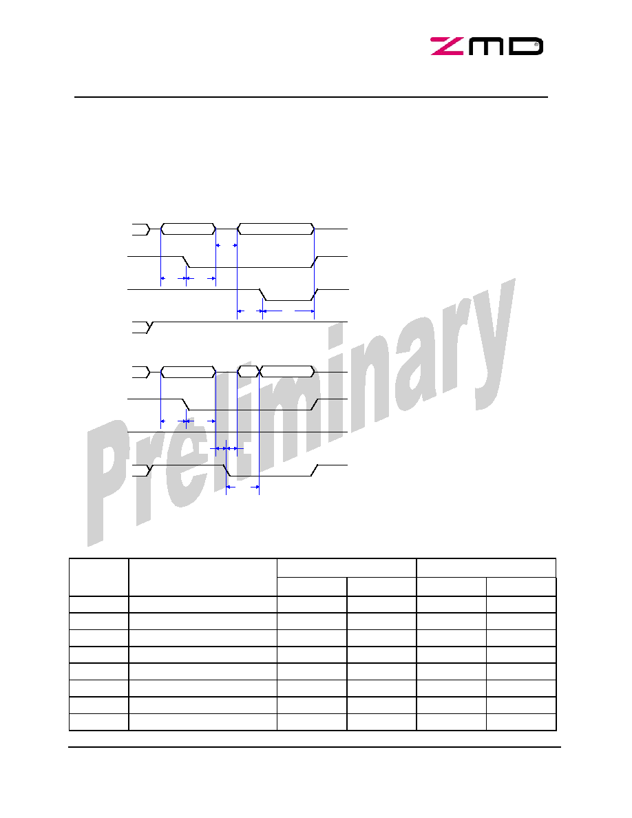
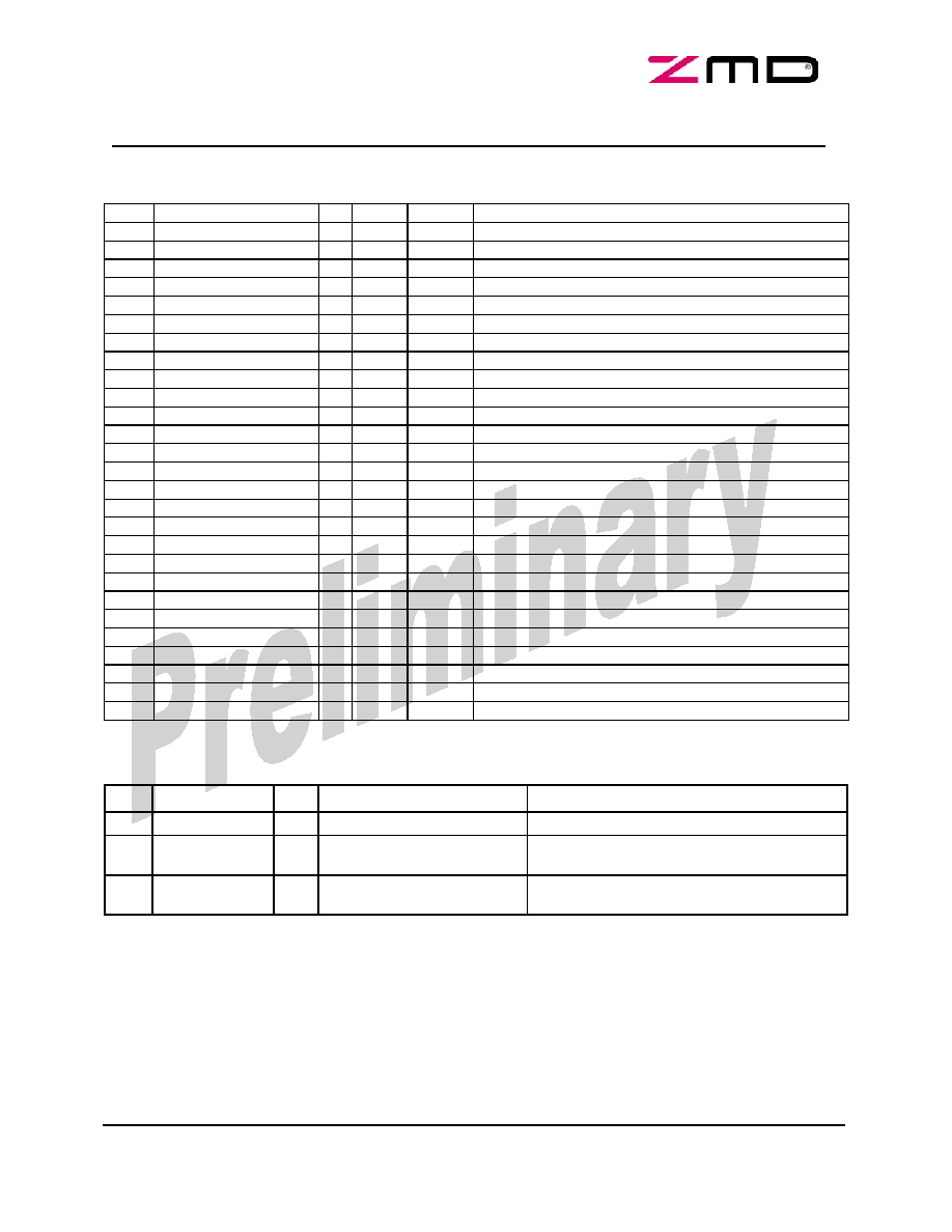
Address
DA[7:0]
RD
WR
ALE
tas
tah
tad
tds
Write Data
tdh
write access:
read access:
Address
DA[7:0]
RD
WR
ALE
tas
tah
Read Data
X
tar
tzd
trvd
4.3 Parallel
Interface
The parallel interface consists of the bi-directional DataAddress[7:0] bus and the control inputs read (RD),
write (WR) and address latch enable (ALE). The direction of the DA[7:0] bus is controlled by the RD input.
If RD is high DA[7:0] are in input mode. Setting RD low turns DA[7:0] into output direction.
The timing diagram for read and write access is shown below.
Figure 4-2: Parallel Interface Read/Write Access
Timing parameters are listed in the following table.
US mode
EU mode
Parameter Description
min
max
min
max
tas
address setup time
0
0
tah
address hold time
200 ns
200 ns
tad
address to data time
0
0
tds
data setup time
0
0
tdh
data hold time
300 us
600 us
tar
address to RD low time
0
0
tzd
high-z to data time
0
10 ns
0
10 ns
trvd
read low to valid data
400 us
800 us
ZMD44101
Single-Chip 868MHz to 928MHz RF Transceiver
P
RELIMINARY - March 2005
Copyright © 2005, ZMD AG
Page 10 of 26
5 Registers
The ZMD44101 has several registers for MAC and PHY functional support. The register description shall
give a brief overview only. A more detailed description can be found in the users manual. The registers are
accessible through the two interface ports. The Hardware-MAC registers provide a great advantage for
system implementation in comparison to a MAC implementation in a microcontroller only. Especially many
system timing critical functions are implemented in the ZMD44101. Most registers can be referred to in the
IEEE802.15.4 standard.
5.1 MAC control + status register
Addr Register
name
bits type default description
8'hE0 IRQreason
8 RW
0
interrupt reason
8'hE1 IRQmask1
8 RW
8'h00
interrupt mask[7:0]
8'hE2 IRQmask2
8 RW
8'h00
interrupt mask[15:8]
8'hE3 IRQmask3
7 RW
7'h00
interrupt mask[22:16]
8'hE4 SPIconfig
6 RWI 6'h20
SPI configuration register
8'hE5 SPIstart
1 RWS
0
SPI start (master mode)
8'hE6 SPItx
8 RW
0
SPI transmit byte (master mode)
8'hE7 SPIrx
8 R
0
SPI receive byte (master mode)
8'hE8 ClkOutConfig
8 RW
8'h29
CLKO pad configuration (def: normal mode = 24Mhz/4,
sleep mode = 32.768kHz)
8'hF0 macControl
5 RW
5'h1F
MAC control command used by firmware to control the
HW-MAC fsm transitions this control word is cleared by
the internal logic after it was fetched 8'hF3
8'hF1 macTxConfig
4 RW
4'h2
MAC transmit mode configuration
8'hF2 macRxConfig
6 RW
6'h1A
MAC rx mode configuration
8'hF3 macBcTrConfig
4 RW
4'h1
MAC beacon track mode configuration
8'hF4 macScanMode
2 RW
0
MAC scan mode (ed, passive, active, orphan)
8'hF5 macOpMode
4 R
0
MAC
operating mode status register
8'hF6 macTxStatus
7 R
0
MAC transmit status register
8'hF7 macRxStatus
8 R
0
MAC rx status register
8'hF8 macScanStatus
8 R
0
MAC scan status register
8'hF9 macBcTrStatus
4 R
0
MAC beacon track status register
8'hFA macAutoBcTxStatus
3 R
0
MAC auto beacon tx status register
8'hFB macFifoStatus
4 R
0
MAC tx/rx fifo status register
ZMD44101
Single-Chip 868MHz to 928MHz RF Transceiver
PRELIMINARY
-
March 2005
Page 11 of 26
Copyright © 2005, ZMD AG
5.2 MAC timing registers
Addr Register
Name
bits
type default description
8'hC0 T_RxDefer1
8 RW
8'h00
rx defer time [7:0]
8'hC1 T_RxDefer2
8 RW
8'h00
rx defer time [15:8]
8'hC2 T_RxDefer3
8 RW
8'h00
rx defer time [23:16]
8'hC9 T_ScanDuration1
8 RW
8'h00
scan duration (960*2^5) [7:0]
8'hDA T_ScanDuration2
8 RW
8'h78
scan duration (960*2^5) [15:8]
8'hCB T_ScanDuration3
8 RW
8'h00
scan duration (960*2^5) [23:16]
8'hCC T_BeaconInterval1
8 RW
8'h00
beacon interval (960*2^5) [7:0]
8'hCD T_BeaconInterval2
8 RW
8'h78
beacon interval (960*2^5) [15:8]
8'hCE T_BeaconInterval3
8 RW
8'h00
beacon interval (960*2^5) [23:16]
8'hCF
Td_BeaconInterval
4
RW 4'h4 T delta beacon interval generate IRQ
2^Td_BeaconInterval before next beacon
8'hD0 T_BeaconScanDuration1 8 RW
8'h00
beacon scan duration (960*2^6) [7:0]
8'hD1 T_BeaconScanDuration2 8 RW
8'hF0
beacon scan duration (960*2^6) [15:8]
8'hD2 T_BeaconScanDuration3 8 RW
8'h00
beacon scan duration (960*2^6) [23:16]
8'hD3 T_BeaconScanStart1
8 RW
8'h0A
beacon scan start (symbols before beacon interval end)
(10) [7:0]
8'hD4 T_BeaconScanStart2
3 RW
3'h0
beacon scan start (symbols before beacon interval end)
(10) [10:8]
8'hD5 T_Sleep1
8 RW
8'h00
sleep time [7:0]
8'hD6 T_Sleep2
8 RW
8'h00
sleep time [15:8]
8'hD7 T_Sleep3
8 RW
8'h00
sleep time [23:16]
8'hD8 Tdelta1
8 RW
0
superframe timing deviation between RFD and FFD [7:0]
8'hD9 Tdelta2
3 RW
0
superframe
timing
deviation between RFD and FFD [10:8]
used as additional guard time in CAP/GTS check
8'hDA SFalignOrder
4 RW
4'h0C
superframe timing alignment order the RFD superframe
timer is aligned to the estimated FFD timing every
60*2^SFalignOrder symbols (12)
ZMD44101
Single-Chip 868MHz to 928MHz RF Transceiver
P
RELIMINARY - March 2005
Copyright © 2005, ZMD AG
Page 12 of 26
5.3 Other MAC registers
Addr Register
name
bits
type default description
8'h9D msduLengthTx
7 RW
0
MAC payload (msdu) length (Tx)
8'hA0 mhrFc1Rx
8 R
0
MAC header frame control byte 1 (Rx - last received frame)
8'hA1 mhrFc2Rx
8 R
0
MAC header frame control byte 2 (Rx - last received frame)
8'hA2 mhrSquNbRx
8 R
0
MAC header sequence number (Rx - last received frame)
8'hA3 mpduLengthRx
7 R
0
mpdu length (Rx - last received frame)
8'hA6 macFramePend
6 RW
0
number of frames pending in Rx FIFO queue, reset by
software
8'hA7 macSuperframeOrder
4 RW
5
MAC superframe order (SO)
8'hA8 macCAPend
4 RW
15
last slot in CAP
8'hA9 macGTSstart
4 RW
10
1st slot of the GTS
8'hAA macGTSlength
4 RW
0
GTS
length in slots (zero no GTS)
8'hAB macTotalTimeFFD1
8 R
0
current
totaltime
[7:0] (FFD mode) in multiple of 32kHz clock
8'hAC macTotalTimeFFD2
8 R
0
current totaltime [15:8] (FFD mode)
8'hAD macTotalTimeFFD3
8 R
0
current totaltime [23:16] (FFD mode)
8'hAE macTotalTimeRFD1
8 R
0
current totaltime [7:0] (RFD mode)
8'hAF macTotalTimeRFD2
8 R
0
current totaltime [15:8] (RFD mode)
8'hB0 macTotalTimeRFD3
8 R
0
current totaltime [23:16] (RFD mode)
8'hB1 macCurrentSymbolTime1 8 R
0
current superframe time [7:0]
8'hB2 macCurrentSymbolTime2 8 R
0
current superframe time [15:8]
8'hB3 macCurrentSymbolTime3 8 R
0
current superframe time [23:16]
8'hB4 MacCurrent Slot
4 R
0
current slot
8'hB5 macBeaconRxTime1
8 R
0
timestamp[7:0] of the last received beacon
8'hB6 macBeaconRxTime2
5 R
0
timestamp[12:8] of the last received beacon
8'hB7 macScanED
8 R
0
maximum ED value from the ED scan
8'hBE macMaxLostBeacons
4 RW
4
number of max lost beacons before a SyncLoss is indicated
8'hBF macSyncLoss
4 R
4
number of lost beacons
8'h75 CRCfail1
8 R
0
number of CRC failures [7:0]
8'h76 CRCfail2
6 R
0
number
of CRC failures [13:8]
8'h77 FrameRxCount1
8 R
0
number of received frames [7:0]
8'h78 FrameRxCount2
6 R
0
number
of received frames [13:8]
ZMD44101
Single-Chip 868MHz to 928MHz RF Transceiver
PRELIMINARY
-
March 2005
Page 13 of 26
Copyright © 2005, ZMD AG
5.4 MAC header registers
Addr. Register name
bits type
default description
8'h82 mhrFc1Tx
8 RW
0
MAC header frame control byte1(low byte) (Tx)
8'h83 mhrFc2Tx
8 RW
0
MAC header frame control byte2(high byte) (Tx)
8'h84 mhrSquNbTx
8 RW
0
MAC header sequence number (Tx)
8'h85 mhrDstPanId1Tx
8 RW
0
MAC header dest. pan identifier byte1(low byte) (Tx)
8'h86 mhrDstPanId2Tx
8 RW
0
MAC header dest. pan identifier byte2(high byte)(Tx)
8'h87 mhrDstAddr16_1Tx
8 RW
0
MAC header dest. 16bit address byte1(low byte) (Tx)
8'h88 mhrDstAddr16_2Tx
8 RW
0
MAC header dest. 16bit address byte2(high byte) (Tx)
8'h89 mhrDstAddr64_1Tx
8 RW
0
MAC header dest. 64bit address byte1(low byte) (Tx)
8'h8A mhrDstAddr64_2Tx
8 RW
0
MAC header dest. 64bit address byte2 (Tx)
8'h8B mhrDstAddr64_3Tx
8 RW
0
MAC header dest. 64bit address byte3 (Tx)
8'h8C mhrDstAddr64_4Tx
8 RW
0
MAC header dest. 64bit address byte4 (Tx)
8'h8D mhrDstAddr64_5Tx
8 RW
0
MAC header dest. 64bit address byte5 (Tx)
8'h8E mhrDstAddr64_6Tx
8 RW
0
MAC header dest. 64bit address byte6 (Tx)
8'h8F mhrDstAddr64_7Tx
8 RW
0
MAC header dest. 64bit address byte7 (Tx)
8'h90 mhrDstAddr64_8Tx
8 RW
0
MAC header dest. 64bit address byte8(high byte) (Tx)
8'h91 mhrSrcPanId1Tx
8 RW
0
MAC header source pan identifier byte 1(low byte) (Tx)
8'h92 mhrSrcPanId2Tx
8 RW
0
MAC header source pan identifier byte 2(high byte (Tx)
8'h93 mhrSrcAddr16_1Tx
8 RW
0
MAC header source 16bit address byte 1(low byte) (Tx)
8'h94 mhrSrcAddr16_2Tx
8 RW
0
MAC header source 16bit address byte 2 (Tx)
8'h95 mhrSrcAddr64_1Tx
8 RW
0
MAC header source 64bit address byte 1 (Tx)
8'h96 mhrSrcAddr64_2Tx
8 RW
0
MAC header source 64bit address byte 2 (Tx)
8'h97 mhrSrcAddr64_3Tx
8 RW
0
MAC header source 64bit address byte 3 (Tx)
8'h98 mhrSrcAddr64_4Tx
8 RW
0
MAC header source 64bit address byte 4 (Tx)
8'h99 mhrSrcAddr64_5Tx
8 RW
0
MAC header source 64bit address byte 5 (Tx)
8'h9A mhrSrcAddr64_6Tx
8 RW
0
MAC header source 64bit address byte 6 (Tx)
8'h9B mhrSrcAddr64_7Tx
8 RW
0
MAC header source 64bit address byte 7 (Tx)
8'h9C mhrSrcAddr64_8Tx
8 RW
0
MAC header source 64bit address byte 8(high byte) (Tx)
5.5 PHY
registers
Addr register
name
bits Name
Remarks
8'h00 RPCC
8 phyCurrentChannel
Register
RF channel selection
8'h05 RTXM
6
Transmitter Mode Register
Transmitter baseband filtering, output port select,
and PA output level controls
8'h0E RAGCL
8
AGC Level Register
Indicates AGC level in closed loop mode and sets
AGC gain in open loop mode
The system description in paragraph 8 gives information about the registers in the PHY. Many more
registers can be accessed and programmed/read but are not essential for typical applications. All PHY
registers are written through MAC commands as defined in the IEEE802.15.4 standard. They can be
overridden. All PHY registers are read and write capable. Every register can be written to and read from at
any time during operation by the microcontroller through either the parallel or SP Interface. A detailed
description of all register will be available as an application note.

ZMD44101
Single-Chip 868MHz to 928MHz RF Transceiver
P
RELIMINARY - March 2005
Copyright © 2005, ZMD AG
Page 14 of 26
Q1
C1
C2
C6
C7
C8
R2
R1
ZMD44101
1
48
12
13
24
25
36
37 WR
RD
DVDD_3.3
DVSS
DVDD
ALE
AVDD
AVSS
RTC1
RTC2
NC
NC
SS
IRQ
GPD
DVDD_3.3
DVDD
RSN
DVDD
NC
NC
AVDD
LPF2
LPF1
MO
SI
MISO
SC
K
DA[
0
]
DA[
1
]
DA[
2
]
DA[
3
]
DA[
4
]
DA[
5
]
DA[
6
]
DA[
7
]
CLK
O
XT
AL
2
XT
AL
1
AV
D
D
RF
O
AV
SS
RF
I
O
AV
SS
AV
D
D
AV
SS
AV
D
D
NC
NC
Q2
C4
C5
SPI
Microcontroller Interface
11
RESET
Interrupt
Power Down
2.4volt
3.3volt
C3
C10
C11
6 Application
circuit
≠ external components
The ZMD44101 requires very few external components allowing for a small module form factor and low
Bill of Material costs. Figure 6.3 depicts which components are required in a typical application. Aside from
these components only a microcontroller, with it's external components, is needed. This microcontroller
has to maintain and control the application specific software dependent functions as defined by the
Zigbee
TM
standard. The standard microcontroller interfaces are described in paragraph 4.3.
Figure 6.1 - external components in a typical ZMD44101 application
component value
component value
C1
15pF, 5%, SMD
C8
15pF, 5%, SMD
C2
15pF, 5%, SMD
C10
>100uF II 100nF, 6.3v, decoupling
C3
22pF, 5%, SMD
C11
>100uF II 100nF, 6.3v, decoupling
C4
43pF, 5%, SMD
R1
12kOhm, 5%, SMD
C5
43pF, 5%, SMD
R2
3.9kOhm, 5%, SMD
C6
5.6pF, 5%, SMD
Q1
32.768kHz, watch crystal type
C7
220pF, 5%, SMD
Q2
24MHz, ±40ppm
ZMD44101
Single-Chip 868MHz to 928MHz RF Transceiver
PRELIMINARY
-
March 2005
Page 15 of 26
Copyright © 2005, ZMD AG
7 ZMD44101 System Performance Summary
Note: Simulated system performance based on IEEE 802.15.4 standard.
Parameter Value
Operational Specifications
Supply Voltage
+2.2V to +2.7V (typical +2.4V)
Digital IO Voltage
+3.0V to +3.6V (typical +3.3V)
Temperature Range
-40∞C to +85∞C
Frequency of Operation
868MHz to 870MHz (EU) and 902MHz to 928MHz (US)
Typical Supply Current (TX)
32mA
Typical Supply Current (RX-synchronization)
31mA
Typical Supply Current (RX-normal)
28mA
Typical Supply Current (sleep mode)
2µA
System Specifications
Standard Basis
IEEE 802.15.4/D18 Compliant
Spreading Technique
Direct Sequence Spread Spectrum (DSSS)
Modulation Type
Binary Phase Shift Keying (BPSK)
Data Rate Burst
20kBits/s (EU) and 40kBits/s (US)
PN Code
15-chip m-sequence
Processing Gain
12dB
Chip Rate
300kBit/s (EU) and 600kBit/s (US)
RF Bandwidth
600kHz (EU) and 1200kHz (US)
RF Channel Spacing
2MHz (IEEE 802.15.4 compliant)
Overall Crystal Accuracy
±40ppm
Architecture
Receiver (RX)
Direct Down-Conversion
Transmitter (TX)
Direct Up-Conversion
Phase Locked Loop (PLL)
Sigma-Delta Fractional-N
Block Specifications
RF_PLL Frequency Resolution
732Hz
TX Output Power
0dBm (to 50)
TX Spurious Emissions
ETSI (EN 300 220) and FCC (Part 15) compliant
RX Sensitivity
-100dBm@PER<1%
RX Maximum Usable Input Level
-20dBm
RX Selectivity/Blocking Performance
IEEE 802.15.4 Compliant + ETSI RX Class 2
General Parameters
Package 48-pin
QFN
(=MLF
TM
MicroLeadFrame)
ESD Protection
>2kV (Human Body Model ≠ HBM)
Interface
SPI and Parallel
External Components
24MHz & 32.768kHz XTAL, PLL loop filter (RC), Antenna, Microcontroller
Process Technology
0.25µm CMOS
ZMD44101
Single-Chip 868MHz to 928MHz RF Transceiver
P
RELIMINARY - March 2005
Copyright © 2005, ZMD AG
Page 16 of 26
ADC
LP Filter
AGC with LPF
LNA
I
Q
RX
RF PLL
TX
DAC
PA
Mixer
XTAL
OSC
Frequency
Doubler
PFD
90
0M
H
z
48MHz
24MHz
24MHz
D
i
g
i
t
a
l
P
a
r
t
Digital Part
ADC
Master
Bias
LPF
XTAL OSC
32.768kHz
POR
Channel
Gain
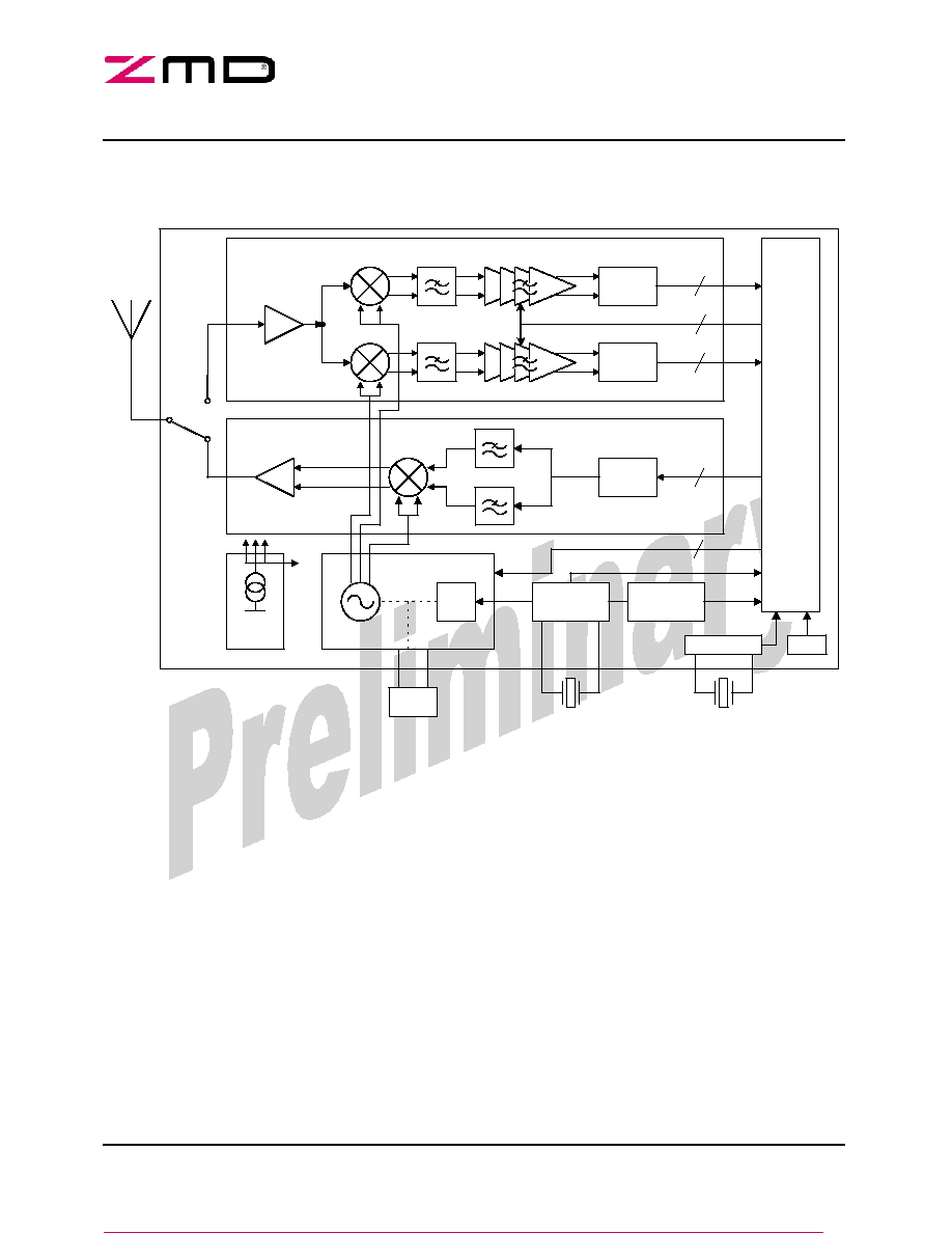
8 System
Description
8.1 General Block Diagram
Figure 8.1 - Integrated Analog PHY Layer block diagram
ZMD44101
Single-Chip 868MHz to 928MHz RF Transceiver
PRELIMINARY
-
March 2005
Page 17 of 26
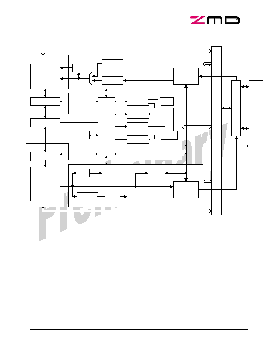
Copyright © 2005, ZMD AG
MAC Control
PHY RX
MAC RX
PHY TX
MAC TX
Reg.
Bank
TX Data Path
- phy frame
- byte to bit
- diff. encode
- spreading
- pulse shape
RX Data Path
- ED
- carrier sense
- acquisition
- notch
- down convert
- despread
- diff. demod
- bit to byte
PHY TX Control
PHY RX Control
Power Control
TX FIFO/
RX FIFO(2)
RX FIFO(1)
CRC
CRC
MAC
Control
RTC
Beacon/Sync
Timing
GTS
Timing
Inter
face
SPI
Parallel
CSMA
IRQ
MAC
Framer
Symbol
Timer
Scan
Timing
Header
Decode
AckReq,
SeqNum,
FrameType
Clock Control
GPD
Bad Frame
Counter
Ack
Frame
PER/BER
Figure 8.2 - Integrated digital PHY and MAC Layer block diagram
8.2 Receiver
Chain
The receiver of the ZMD44101 uses a direct-conversion architecture (Zero-IF architecture).
The receiver path consists of a 900MHz low-noise amplifier (LNA) and a mixer, followed by the analog
baseband. It contains multi-stage programmable gain amplifiers, low-pass filter sections and Analog-to-
digital converters (ADC). All remaining functions are carried out in the digital domain including
synchronization, de-spreading and demodulation as well as the AGC loop control. To extend the dynamic
range further, the LNA and mixer gain can be adjusted in the AGC loop.
In normal operation mode, the user or the MAC starts the reception using the default register values. All
control signals (timing, power-down) are set automatically.
One receiver register setting can be important for receiver operation (RAGCL). This is described in
paragraph 8.2.1. Besides this register there are registers which are used in both, transmit and receive
mode.
ZMD44101
Single-Chip 868MHz to 928MHz RF Transceiver
P
RELIMINARY - March 2005
Copyright © 2005, ZMD AG
Page 18 of 26
8.2.1 RAGCL - AGC Level Register
Bit7 Bit6 Bit5 Bit4 Bit3 Bit2 Bit1 Bit0
0 1 1 1 1 1 1 1
1=gain high, 0=gain low
The register can be used to read the AGC level back to the microcontroller at any time during receiver
operation. This way information about the signal strength can be derived by the microcontroller. The high
gain default value (hex7F) together with the digital peak detection function ensures fast settling time by
reducing the gain in steps to a usable signal level for the digital signal processing inside the ZMD44101.
8.3 Transmitter
Chain
A direct-conversion architecture is used for the transmitter of the ZMD44101. The design is fully
differential. Only the Power Amplifier (PA) output is single-ended. No external balun is required.
In normal operation mode, the user or the MAC starts the transmission using the default register values.
All control signals (timing, power-down) are set automatically.
Optionally two default register settings of the transmitter can be changed by writing to the Transmitter
Mode Register (RTXM). By default, the PA drives 0dBm (1mW) to a 50 Ohm off-chip load. This output
power can be changed between 0dBm and -21dBm.
8.3.1 RTXM - Transmitter Mode Register
Bit7 Bit6 Bit5 Bit4 Bit3 Bit2 Bit1 Bit0
default
0 0 0 0 0 0 0 0
0 dBm output power
0
0
0
0
X
X
X
X
-7 dBm output power
0
0
0
1
X
X
X
X
-14 dBm output power
0
0
1
0
X
X
X
X
-21 dBm output power
0
0
1
1
X
X
X
X
Normal
operation
0 0 X X X 0 0 0
Carrier only modulation
0
0
X
X
X
0
1
0
Constant '0' data transmit
0
0
X
X
X
1
0
0
RFIO is output
0
0
X
X
0
X
X
X
RFO is output
0
0
X
X
1
X
X
X
ZMD44101
Single-Chip 868MHz to 928MHz RF Transceiver
PRELIMINARY
-
March 2005
Page 19 of 26
Copyright © 2005, ZMD AG
TX-RX-Switch Configuration
RXIO
RFIO
TXIO
RFO
TXO
LNA
PA
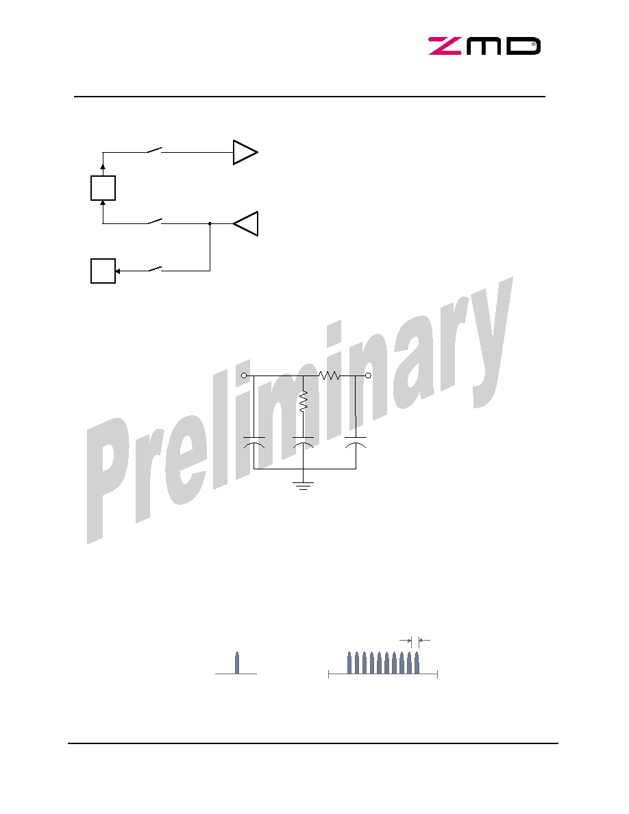
Furthermore, by default the receiver input and
the transmitter output use the same pin (RFIO).
The integrated antenna switch disconnects the
respective components in transmit and receive
mode.
By changing bit3 in the RTXM register, the
transmitter uses RFO as the output pin. This
allows to use an external Power Amplifier for
higher output power and extended range (see
left figure).
The antenna has to be connected via an
external 22pF capacitor.
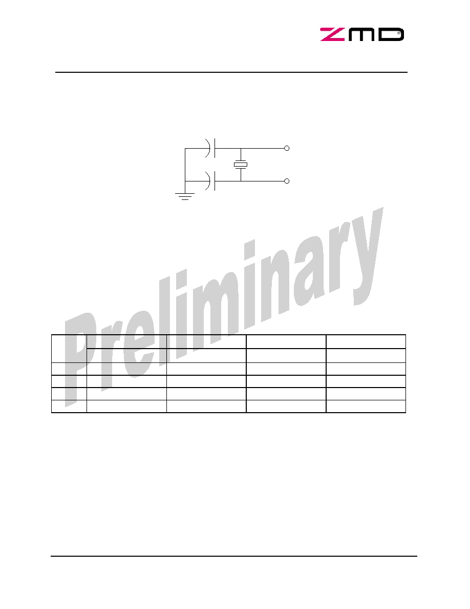
8.4 RF Phase Locked Loop
A fractional-N Phase Locked Loop (PLL) architecture is used. All functions are integrated on chip except
for the loop filter. The external loop filter circuitry is depicted in Figure 8.3. The 24MHz crystal (see
paragraph 8.5) provides the reference frequency for both the EU- and US-bands.
5.6pF 5%
220pF 5%
15pF 5%
3.9k 5%
12k 5%
LP_CP
LP_VCO
Figure 8.3 - PLL-Loop filter
In normal operation mode, the user sets the frequency channel of the RF PLL prior to transmission or
reception. All control signals (timing, power-down) are set automatically by writing to the
phyCurrentChannel register (RPCC), but can be overwritten for non-standard applications. The data rate
(EU: 20kBit/s and US: 40kBit/s) is adjusted automatically according to the selected channel. The channel
numbers are defined by the IEEE 802.15.4 standard. Figure 8.4 illustrates the channel allocation in the
900MHz band. Table 8.1 depicts the RPCC programming in the ZMD44101.
868.3 MHz
Channel 0
Channels 1-10
928 MHz
902 MHz
2 MHz
Figure 8.4 - Channel allocation in the 900MHz band

ZMD44101
Single-Chip 868MHz to 928MHz RF Transceiver
P
RELIMINARY - March 2005
Copyright © 2005, ZMD AG
Page 20 of 26
Band Channel
select
(RPCC Reg.)
as per IEEE802.15.4
Channel
(MHz)
Channel (bin)
(RPLC1/2 Reg.)
Channel (dec)
SEL_SUBBAND
(RPLM Reg.)
European 0 868.3
0010110111011101
11741
01
USA 1
906
1100000000000001
49153
10
USA 2
908
1101010101010101
54613
10
USA 3
910
1110101010101011
60075
10
USA 4
912
0000000000000000
0
11
USA 5
914
0001010101010101
5461
11
USA 6
916
0010101010101011
10923
11
USA 7
918
0100000000000001
16385
11
USA 8
920
0101010101010101
21845
11
USA 9
922
0110101010101011
27307
11
USA 10
924
1000000000000001
32769
11
Table 8.1 ≠ Channel select register programming according to the IEEE 802.15.4 standard
8.5 Reference Crystal Oscillator (24MHz)
A two (2) pin Pierce oscillator with on-chip biasing resistor is designed to provide the necessary reference
frequency at 24MHz. This frequency is used for digital clock supply, timing calculations as well as for the
PLL that generates the RF carrier frequency. For the receive modes the internal circuitry doubles the
reference frequency in order to achieve the digital processing speed during code acquisition. This
oscillator is only active in Idle, Transmit and Receive power modes.
The user can also provide an external 24MHz clock reference on XTAL1. This external clock has to have
24MHz at a duty cycle of 1:1 and an accuracy of
±40ppm. Provided this case no 24MHz crystal is required
between XTAL1 and XTAL2 and XTAL2 is not connected.
When the internal oscillator is used C4 and C5 are required as load capacitors for the parallel resonance
crystal. The values C4 and C5 are different for any specific environment. The overall load capacitance is
composed of the actual values of C4 and C5 as well as the parasitic values of the PCB layout and the
internal parasitic capacitance of the ZMD44101, which is 0.65pF on each pin. The total load capacitance
has to match the recommended typical load capacitance provided by the crystal manufacturer. For a
recommended 97SMX240 22B crystal (SMI) the load capacitance is 22pF
±0.5%. Any deviation on this
system part will result in large deviation on the carrier frequency and output spectrum.
This clock is available for external use on Pin 36, CLKO. It can be used to support a microcontroller.
During power-down and sleep mode the microcontroller clock is switched to 32.768kHz or to selectable
fractions of 32.768kHz for reduced current consumption. This ensures the microcontroller has a clock
signal during power-down and therefore can correctly wake up from the power-down state. During all
other states the 24Mhz clock or selectable fractions of 24MHz can be used on CLKO.
XTAL2
XTAL1
24MHz
C4
C5
Figure 8.5 - 24Mhz crystal oscillator ≠ external components
ZMD44101
Single-Chip 868MHz to 928MHz RF Transceiver
PRELIMINARY
-
March 2005
Page 21 of 26
Copyright © 2005, ZMD AG
8.6 Low Power Crystal Oscillator (32.768kHz)
The 32.768kHz crystal oscillator is designed for extreme low power operation as it always runs when
power is applied to the device. The oscillator provides the time reference for the on-chip real time clock.
The oscillator utilizes an amplitude controlled two (2) pin Pierce oscillator with on-chip biasing resistor. The
same as described for the 24MHz oscillator in paragraph 8.5 is valid for the load capacitance.
RTC2
RTC1
32.768kHz
Figure 8.6 - 32.768khz crystal oscillator ≠ external components
This clock is available for external use on Pin 36, CLKO. It can be used to support a microcontroller.
During power-down and sleep mode the microcontroller clock is switched to 32.768kHz or to selectable
fractions of 32.768kHz for reduced current consumption. This ensures the microcontroller has a clock
signal during power-down and therefore can correctly wake up from the power-down state.
8.7 CLKO - Clock Output Configuration
This register is part of the MAC control and status registers. The clock on the CKLO pin can be configured
according to the following table for external microcontroller clock support. Pin36 can directly drive a clock
input up to 4mA.
ClkOutConfig[7:6] ClkOutConfig[5:4] ClkOutConfig[3:2] ClkOutConfig[1:0]
value
RtcDiv(M) Clk24Div(N)
NormalModeClk
SleepModeClk
0 1
1
OFF
OFF
1 2
2
32k/M 32k/M
2 4
4
24M/N 24M/N
3 8
8
The table is to be read as follows. Example default: The ClkOutConfig(@default)=8'b00101001, compares
to "0,2,2,1". That means: M=1, N=4, during normal mode (everything but not sleep or GPD) CLKO is
24MHz/4=6MHz, and during sleep mode CLKO is 32.768kHz.

ZMD44101
Single-Chip 868MHz to 928MHz RF Transceiver
P
RELIMINARY - March 2005
Copyright © 2005, ZMD AG
Page 22 of 26
8.8 Power
Management
The ZMD44101 has five different modes of power management. These modes are user configurable and
controlled by the external microcontroller. The power modes are as follows:
∑ Tx/Rx: Tx or Rx is active.
∑ IDLE: Tx/Rx are powered down but the 24MHz crystal oscillator remains on.
∑ SLEEP: All circuits are switched off except the 32.768kHz RTC for accurate time reference.
Power consumption is reduced to 2µA (typical).
∑ POWER DOWN: The ZMD44101 enters into power down by setting the Global Power Down
(GPD) function.
∑ POWER OFF: The supply voltage is switched off externally. The ZMD44101 has a Power On
Reset (POR) function.
NOTE: The ZMD44101 contains internal master bias circuitry. No adjustments or external circuitry are
required for accurate operation.
ZMD44101
Single-Chip 868MHz to 928MHz RF Transceiver
PRELIMINARY
-
March 2005
Page 23 of 26
Copyright © 2005, ZMD AG
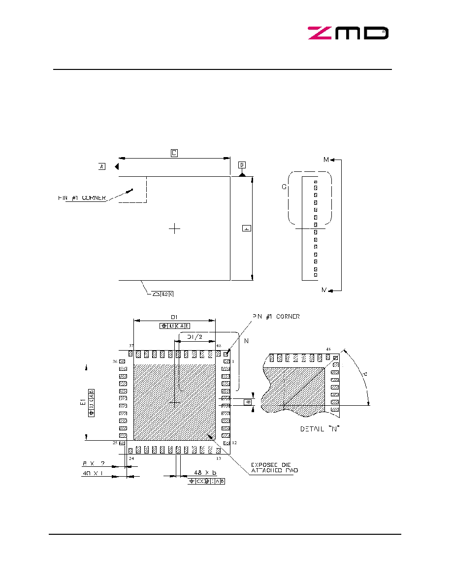
9 Mechanical
Specifications
9.1 Package
48pin QFN Package

ZMD44101
Single-Chip 868MHz to 928MHz RF Transceiver
P
RELIMINARY - March 2005
Copyright © 2005, ZMD AG
Page 24 of 26
Dim Min Typ Max
Notes
A 0.80 1.00
A1 0.203
Ref
b
0.18
0.25
0.30 Applies to metallized terminal and is measured between
0.25mm and 0.30mm from terminal tip.
D 7.00
BSC
E 7.00
BSC
D1 5.04
5.24
E1 5.04 5.24
e 0.50
BSC
L 0.43
0.53
0.63
L1
0.10 Represents terminal full back from package edge up to 0.1mm
is acceptable.
L2 0.30 0.40 0.50
P 45
o
BSC
aaa 0.15
ccc 0.10
Notes:
1. Dimensions and tolerances conform to ASME Y14.5M-1994
2. All dimensions are in millimeters. Angles are in degrees.
3. Co-planarity applies to the exposed head slug as well as the terminal.
4. Radius in terminal is optional.

ZMD44101
Single-Chip 868MHz to 928MHz RF Transceiver
PRELIMINARY
-
March 2005
10 List of abbreviations
ADC
Analog-to-Digital
Converter
AES
Advanced Encryption Standard
AGC
Automatic Gan Control
BER
Bit Error Rate
BPSK
Binary Phase Shift Keying
CMOS
Complementary Metal Oxide
Silicon
CRC
Code Redundancy Check
CSMA
Carrier Sense Multiple Access
DAC
Digital-to-Analog
Converter
dB
Decibel
DSSS
Direct Sequence Spread
Spectrum
ED
Energy
Detection
ESD
Electrostatic
Discharge
ETSI
European Telecommunications
Standards Institute
EU
Europe
FCC
Federal Communications
Commission
FIFO
First In First Out
GPD
General Power Down
GTS
Guaranteed Time Slot
IEEE
Institute of Electrical and
Electronics Engineers
IF Intermediate
Frequency
IRQ
Interrupt
request
ISM
Industrial- Scientific Medical
kbit/s
Kilobit per second
kHz
Kilohertz
LNA
Low
Noise
Amplifier
LoS
Line of sight
LP Filter
Low Pass Filter
MAC
Medium
Access
Controller
MISO
Master-In-Slave-Out,
MOSI
Master-Out-Slave-In
MHz
Megahertz
MLF
Micro Lead Frame
PER
Packet
Error
Rate
PHY
Physical
(Layer)
PLL
Phase Locked Loop
QFN
Quad Flat Pack
RF
Radio
Frequency
RTC
Real Time Clock
RX
Receiver
SPI
Serial Peripheral Interface
SS
Slave-Select (refers to CS=Chip
Select)
TX
Transmitter
US
United
States
XTAL
Crystal
11 References
∑ IEEE 802.15.4-2003 Standard: "IEEE Standard for Part 15.4: Wireless Medium Access Control
(MAC) and Physical Layer (PHY) Specifications for Low Rate Wireless Personal Area Networks (LR-
WPANs)". Download: http://standards.ieee.org/getieee802/download/802.15.4-2003.pdf
∑ ETSI EN 300 220-1 V1.3.1 (2000-09)
∑ FCC Part 15, December 18 2001
Page 25 of 26
Copyright © 2005, ZMD AG

ZMD44101
Single-Chip 868MHz to 928MHz RF Transceiver
P
RELIMINARY - March 2005
The information furnished here by ZMD is believed to be correct and accurate as of the publication date. However, ZMD shall not be
liable to any third party for any damages, including but no limited to personal injury, property damage, loss of profits, loss of use,
interruption of business or indirect, special, incidental, or consequential damages of any kind in connection with or arising out of the
furnishing, performance, or use of the technical data. No obligation or liability to any third party shall arise or flow out of ZMD's
rendering technical or other services.
For
Further
Information
ZMD
Phone: 858-674-8433
Fax: 858-674-8071
e-mail: wireless@zmda.com
ZMD
15373 Innovation Drive
Suite 115
San Diego, CA 92128
http://www.zmd.biz
ZMD AG
Grenzstrasse 28
D-01109 Dresden
Tel.: +49 351 8822 928
Fax: +49 351 8822 666
Products sold by ZMD are covered exclusively by the ZMD standard warranty, patent indemnification, and other provisions appearing
in ZMD standard "Terms of Sale". Testing and other quality control techniques are used to the extent ZMD deems necessary to
support this warranty. Except where mandated by government requirements, testing of all parameters of each product is not
necessarily performed. ZMD makes no warranty (express, statutory, implied and/or by description), including without limitation any
warranties of merchantability and/or fitness for a particular purpose, regarding the information set forth in the Materials pertaining to
ZMD products, or regarding the freedom of any products described in the Materials from patent and/or other infringement.
ZMD reserves the right to discontinue production and change specifications and prices, make corrections, modifications,
enhancements, improvements and other changes of its products and services at any time without notice. ZMD products are
intended for use in commercial applications. Applications requiring extended temperature range, unusual environmental
requirements, or high reliability applications, such as military, medical life-support or life-sustaining equipment, are specifically not
recommended without additional mutually agreed upon processing by ZMD for such applications. ZMD assumes no liability for
application assistance or customer product design. Customers are responsible for their products and applications using ZMD
components.
Print date: 30.03.2005 11:29
Copyright © 2005, ZMD AG
Page 26 of 26